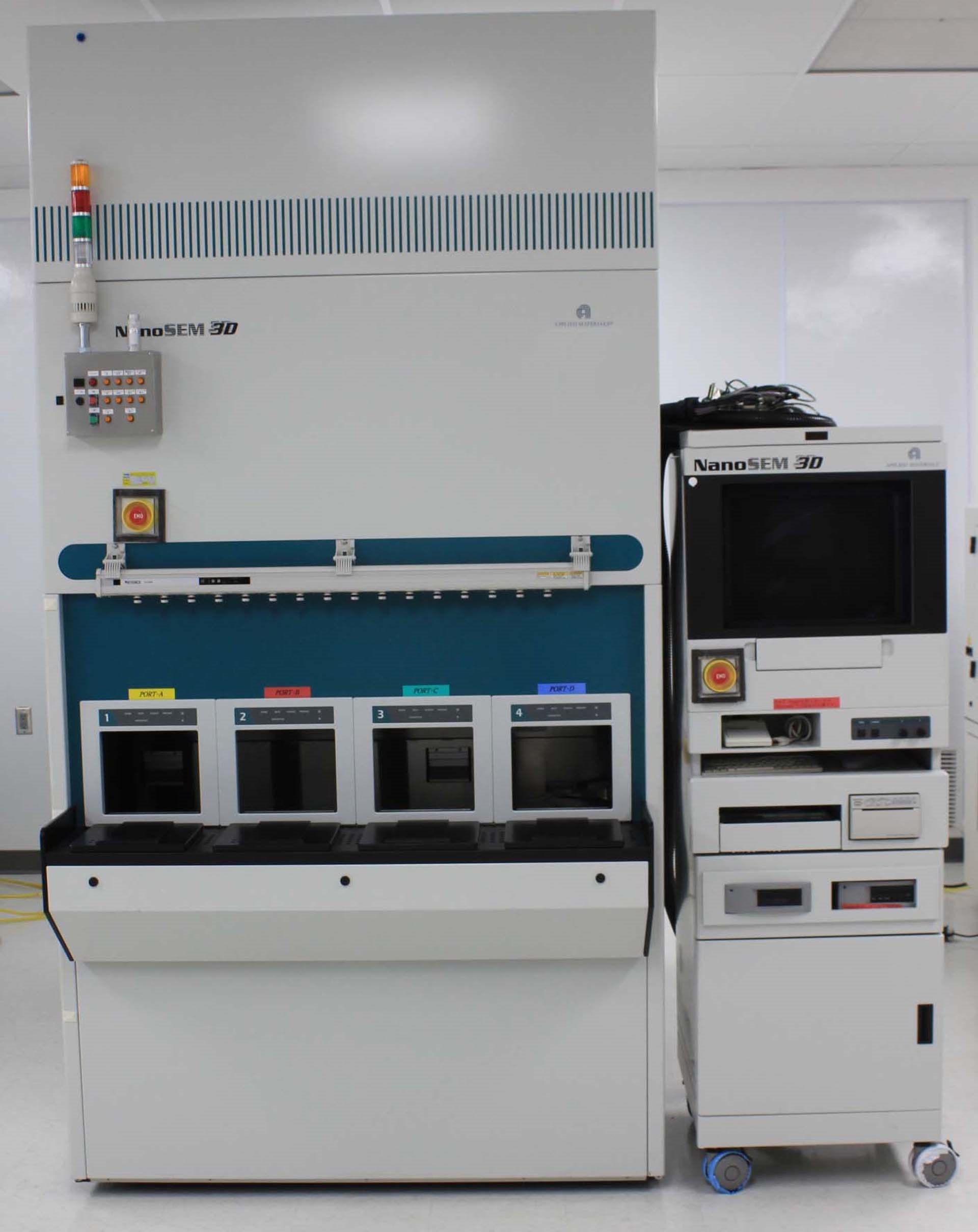
Used AMAT / APPLIED MATERIALS NANOSEM 3D #9138847 for sale
It looks like this item has already been sold. Check similar products below or contact us and our experienced team will find it for you.
Tap to zoom


Sold
ID: 9138847
Wafer Size: 8"-12"
Vintage: 2002
Critical Dimension Scanning Electron Microscope (CD-SEM), 8"-12"
Open cassette
2002 vintage.
AMAT / APPLIED MATERIALS NANOSEM 3D is an advanced wafer testing and metrology equipment designed for use in the semiconductor industry. This system combines the benefits of 3D imaging with dedicated automated features for sample handling and creating critical depth measurements on wafers and other substrates. AMAT NANOSEM 3D unit is capable of measuring depths from 0.1 μm up to several millimeters with a resolution down to 0.01 μm. It is also capable of measuring the contours and roughness of the surface. The machine consists of two main components, the 3D imaging device and the handling tool. The 3D imaging device is based on Digital Imaging Standard (DIS) technology and is capable of recording large image fields while providing high spatial resolution and accuracy. The asset is equipped with a proprietary 3D imaging algorithm that allows for large-scale 3D imaging of objects with different shape, size, and surface morphology. Furthermore, its patented object recognition technology coupled with a variety of head-options enables the model to measure over open cavities and variable planarity. The handling equipment enables automatic sample loading and positioning, and a wide range of manual and automated movement of the imaging head. The automated sample loading process enables quick and accurate loading and positioning of wafers and other substrates. It also supports automated comparison imaging in situations where different wafers need to be analyzed quickly. Furthermore, the system gives full control to the operator, allowing them to interactively adjust the gain and focus settings for improved imaging results. The measuring software for APPLIED MATERIALS NANOSEM 3D unit is easy to operate, allowing for intuitive workflow control and data analysis. It is capable of creating powerful 3D representation of the sample, enabling fast identification and review of topography features. Furthermore, the analysis of the gathered data can provide information on the surface texture and other important dimensions such as radius, slope, and width. In summary, NANOSEM 3D machine is an advanced wafer testing and metrology tool that takes advantage of advanced imaging technology to measure depth and surface profiles with high resolution and accuracy. It features an automated sample handling asset with intuitive software for easy workflow control and data analysis. The model is ideal for the semiconductor industry, enabling fast and accurate imaging of wafers and other substrates.
There are no reviews yet