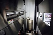
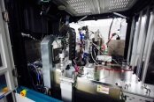
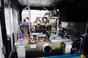
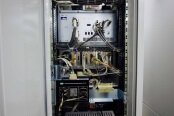
Used AMAT / APPLIED MATERIALS NANOSEM 3D #9280517 for sale
URL successfully copied!
Tap to zoom








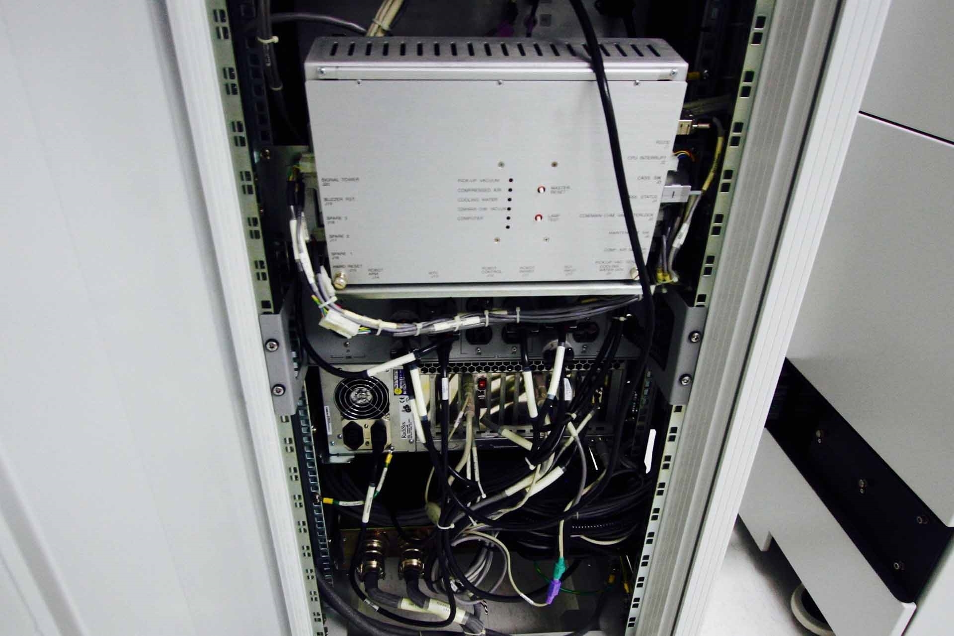

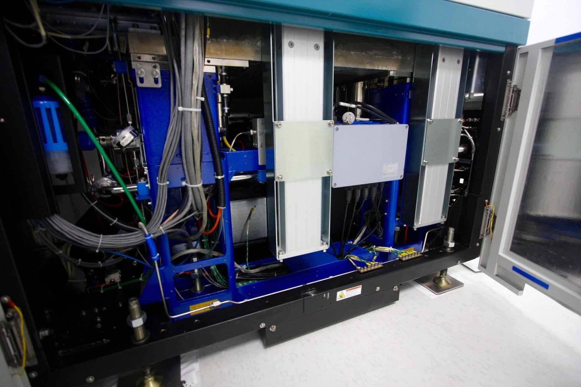

ID: 9280517
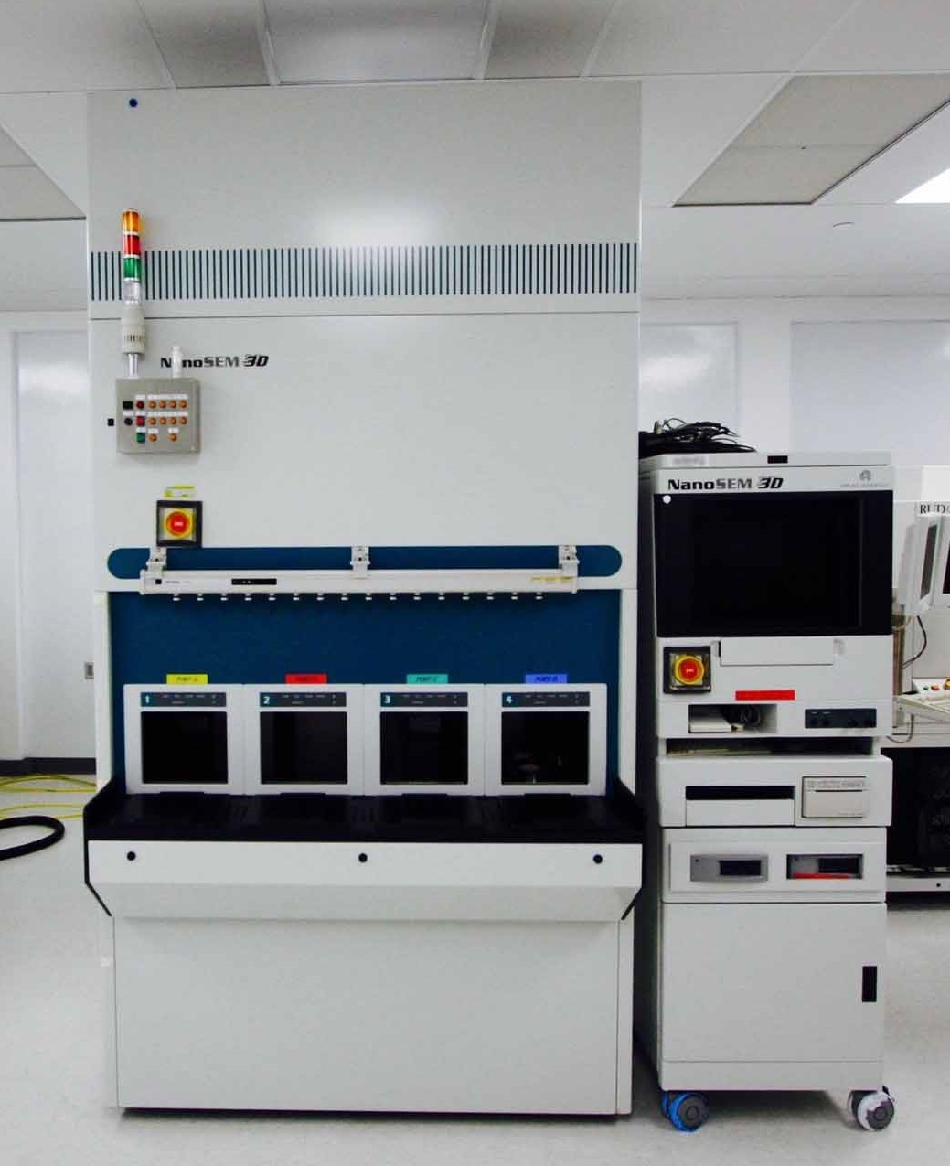
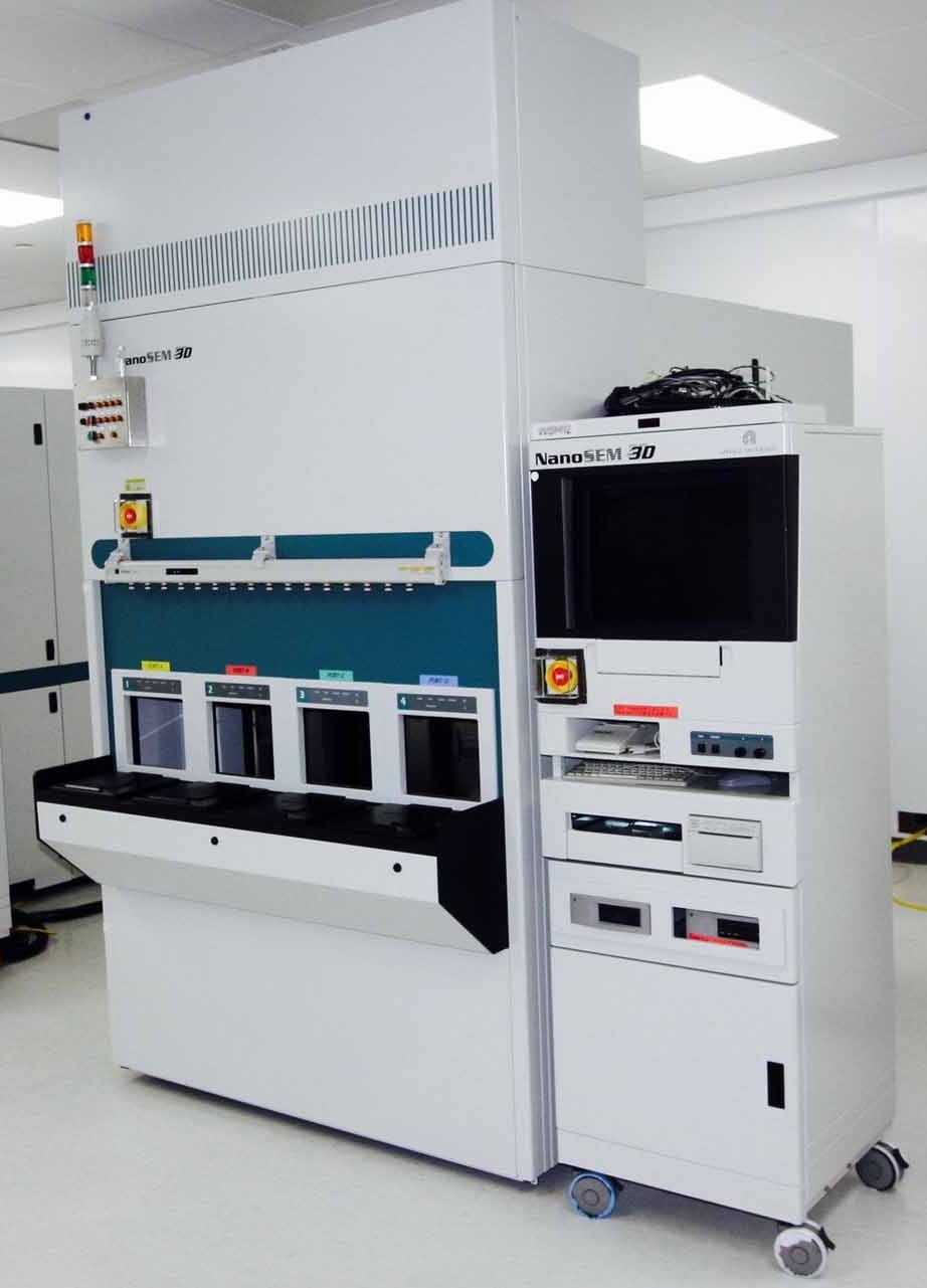
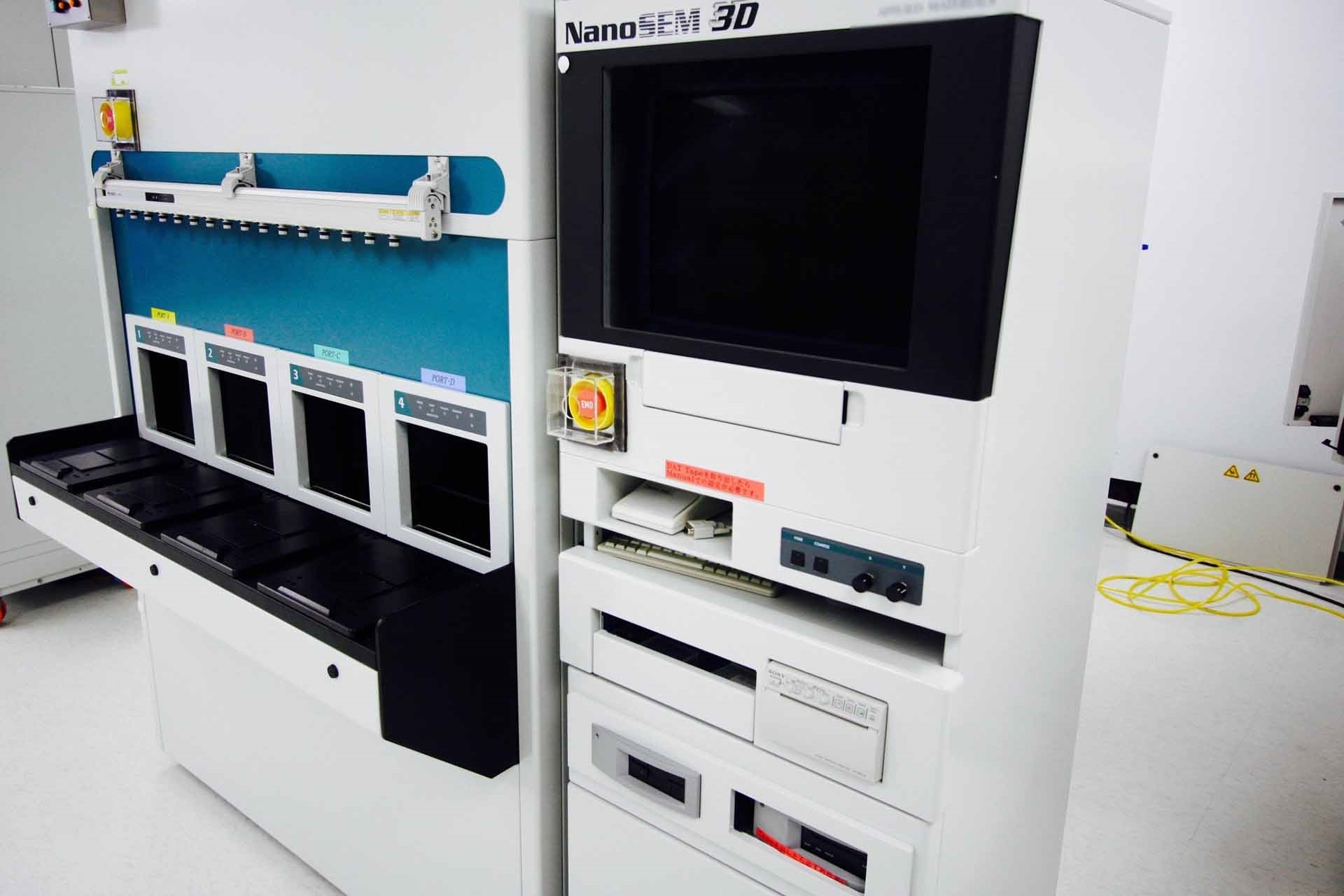
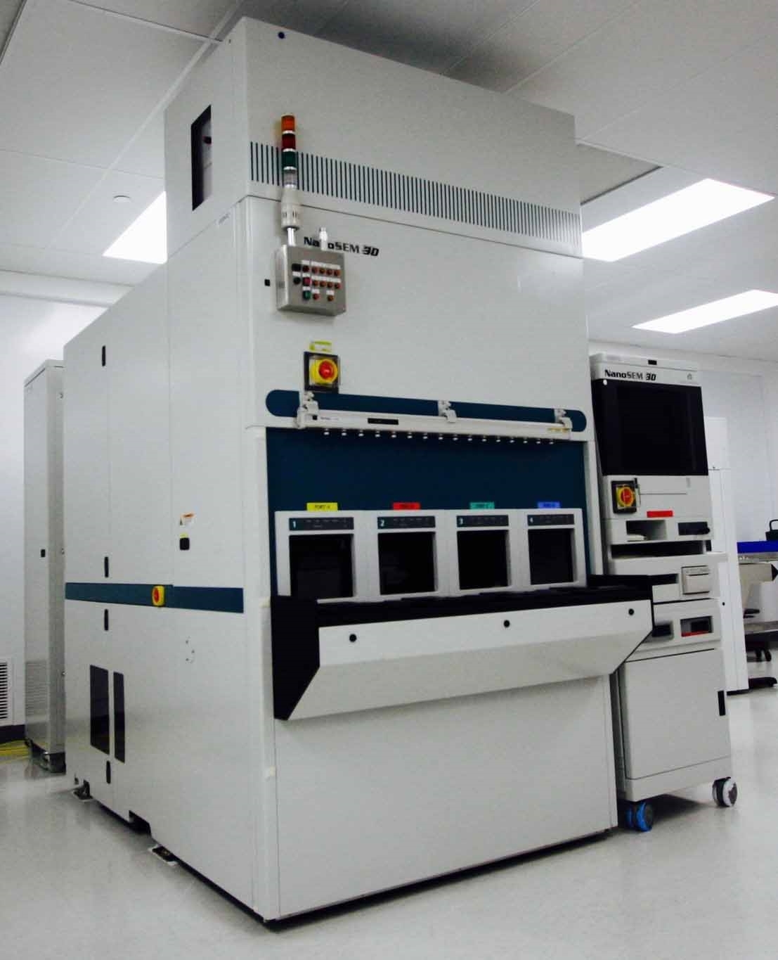
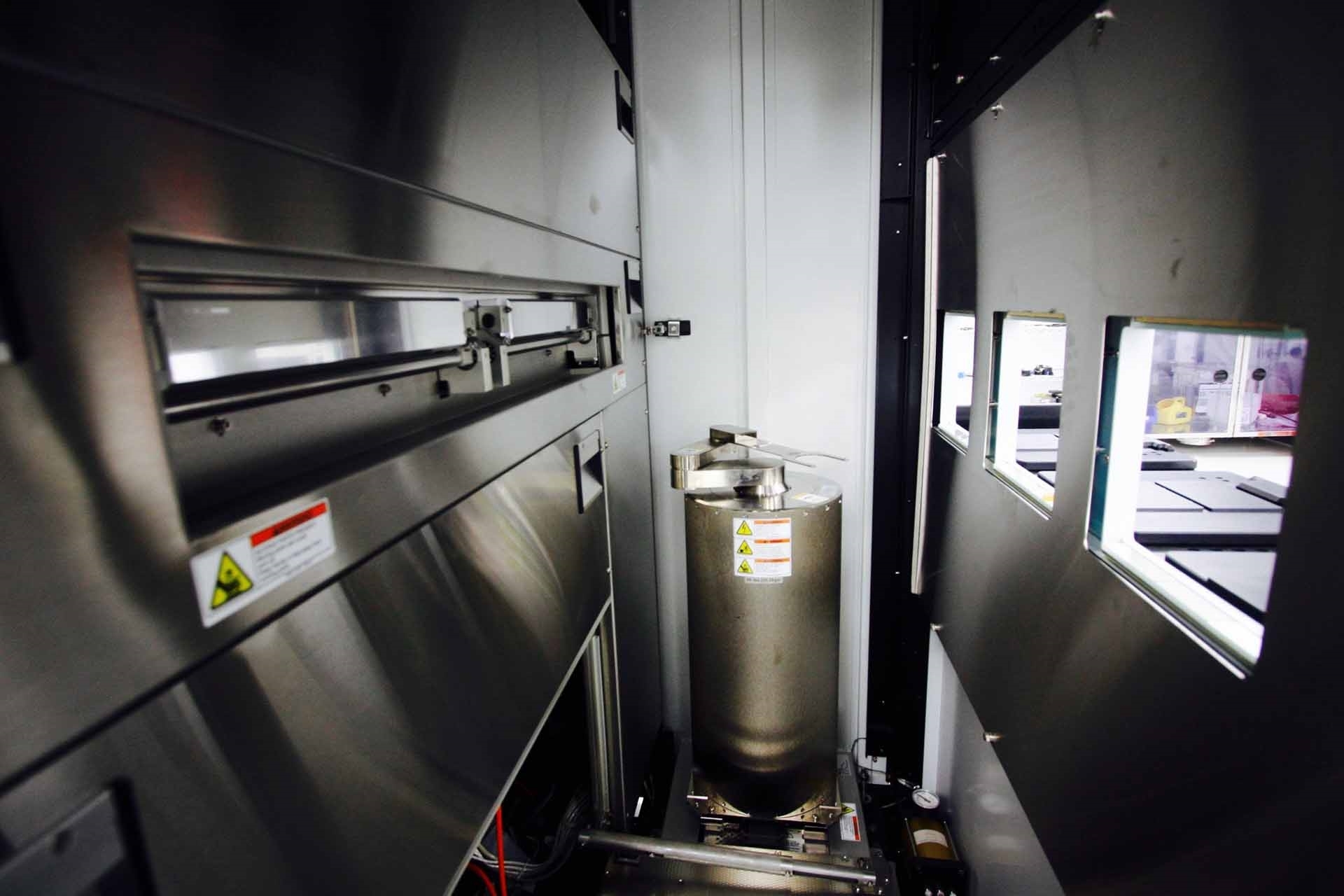
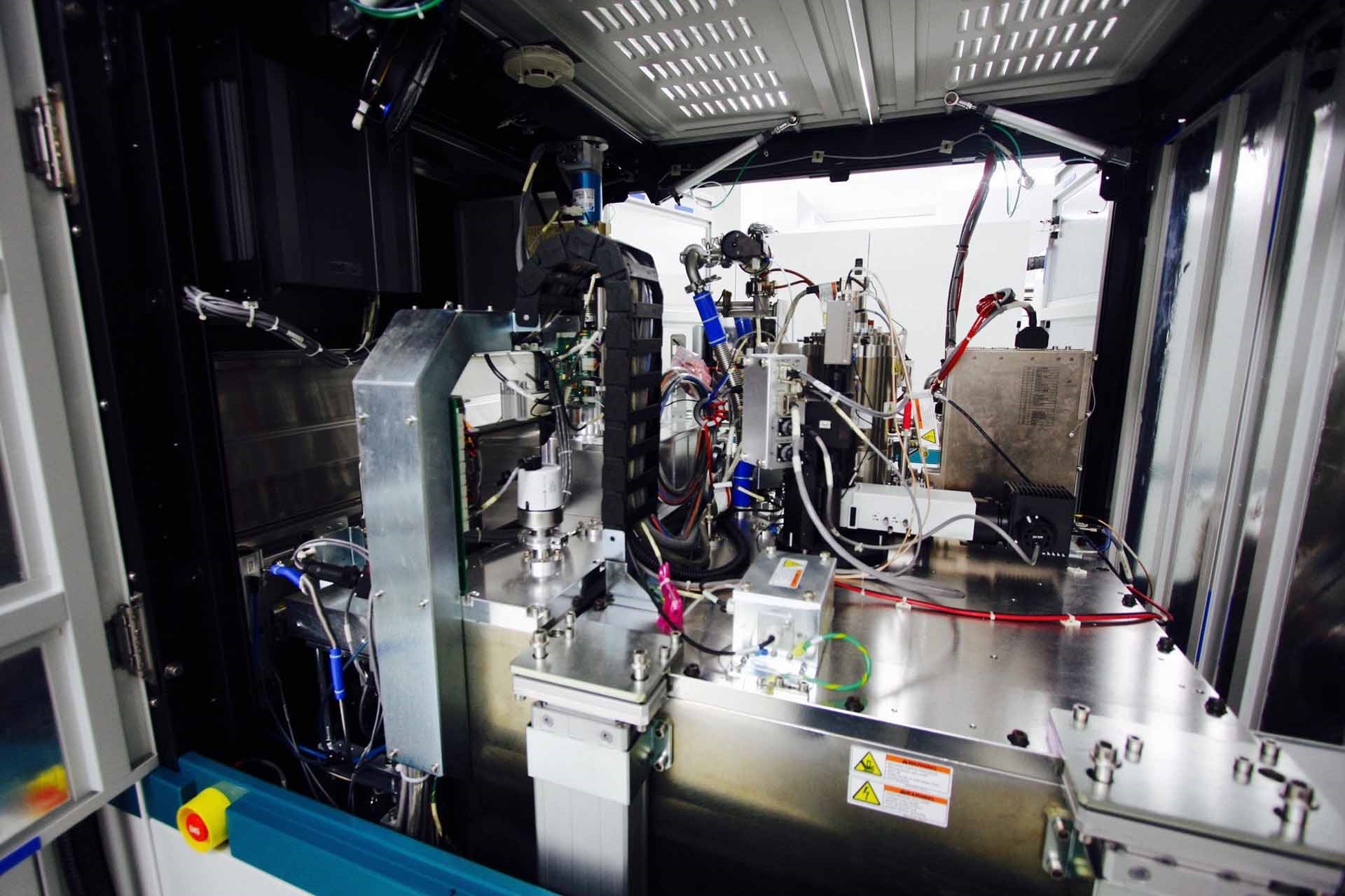
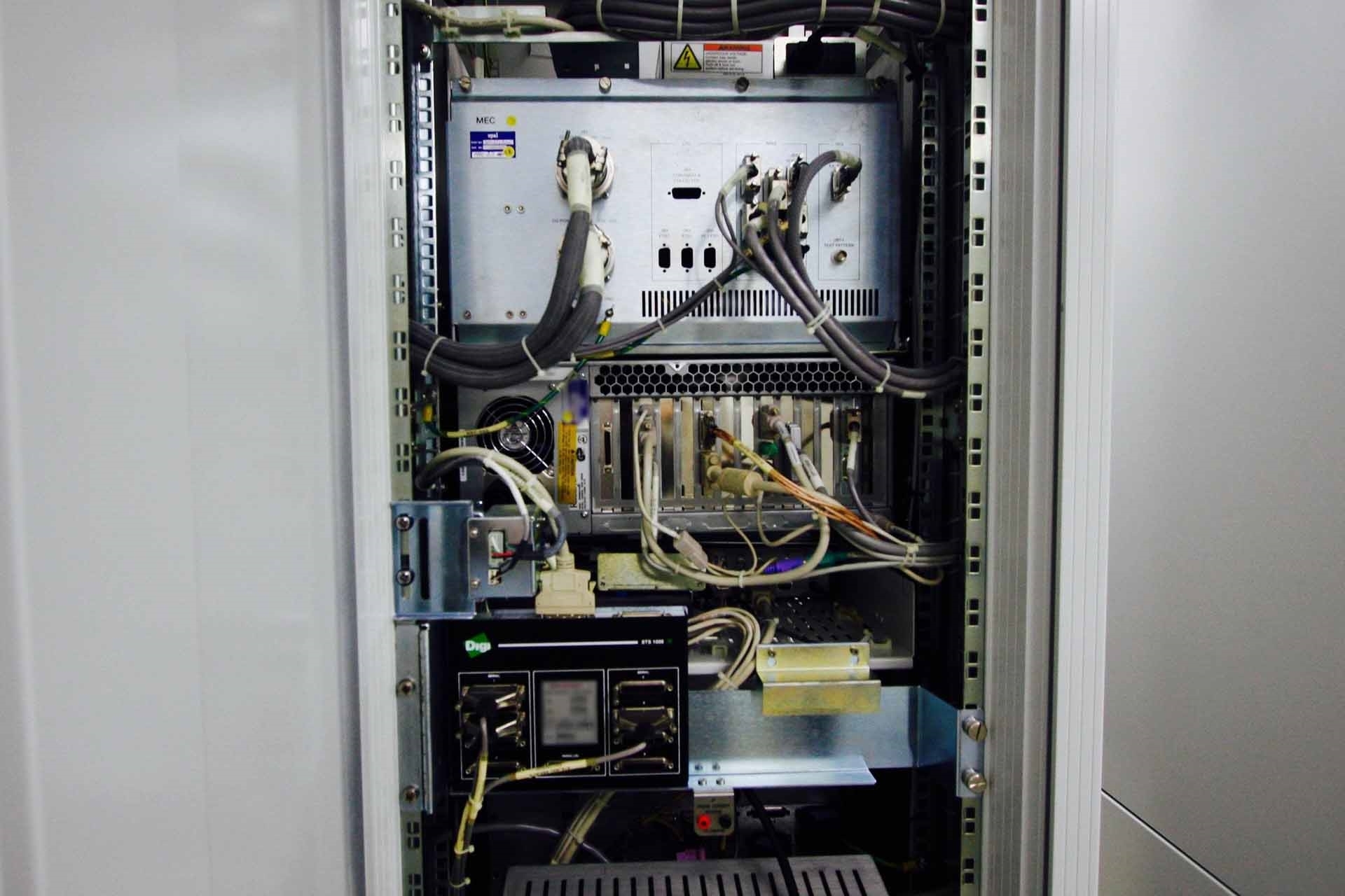
Automated CD metrology system, 8"
Wafer shape: SNNF (Semi Notch No Flat)
Wafer cassette: PP Miraial, 8"
No SMIF Interface
Electron optical system:
Electron gun SCHOTTKY emission source (FEI)
Accelerating voltage: 300 V - 2,000 V
3-Stage Electromagnetic lenses
System with boosting voltage beam deflector module
Objective lens:
Scan coil 2-stage: Electromagnetic deflection (X-axis & Y-axis)
Magnification: 1,000x - 400,000x (100um - 0.25um FOV)
Wafer imaging ability entire surface, 8"
Aspect ratio: >20 : 1
Tilt function: 15° (4 Directions)
Resolution: 2nm (500V)
Optical microscope system:
Camera monochrome: CCD Camera
Magnification: 16x / 220x (450 um / 6000 um FOV)
Wafer imaging ability entire surface, 8"
Workstation:
Model: SGI Octane
OS: Unix
SECS / GEM Communication interface:
Automated image archiving function / Online setup
Measurement function: Contact hole
Line edge analysis / CH Analysis / Slope
Measurement algorithm normal / Foot / Threshold
Wafer stage:
Wafer stage Anorad XY and Z Stage
Moving speed: 300 mm/sec
Function target faraday cup / Resolution target
Wafer transfer:
Wafer shape ability notch / Orientation flat
Pre-alignment sensing by CCD BAR (200/300 mm wafer)
External power distribution unit
Fun filter unit
Prober current:
Low 5pA
Medium 10pA
High 20pA.
AMAT / APPLIED MATERIALS NANOSEM 3D is a high-tech wafer testing and metrology equipment designed to provide unsurpassed accuracy in the characterization of nanotechnology devices. AMAT NANOSEM 3D utilizes cutting-edge, advanced techniques, such as electron-beam standard lithography, 3D imaging, and a non-contact, non-uniformity measurement to enable faster and more accurate device testing. The system features a high-speed multi-beam for constant position control and stable illumination, providing high-quality images with high precision and repeatability. APPLIED MATERIALS NANOSEM 3D utilizes advanced pattern recognition algorithms to identify critical feature parameters in circuit designs. Specialized algorithms analyze feature edges, including edges near contact areas, and can accurately identify feature orientation even if it's reversed. This enhances circuit performance and makes test and measurement times more accurate and efficient. A high-precision, non-contact, non-uniformity measurement unit is included in NANOSEM 3D to ensure uniformity in nanometer-scale features. The machine features a combination of vertical and lateral scanning for C-V characterization, as well as multiple channel capability that can easily be customized for various wafer structures. In order to reduce overhead noise during testing, AMAT / APPLIED MATERIALS NANOSEM 3D includes a unique noise detection and isolation tool. The asset employs advanced pattern recognition algorithms to identify different noises, including thermal and electrical. With this feature, users can quickly detect and isolate any noise-related issues that may arise. AMAT NANOSEM 3D is rugged and customizable for the needs of any production environment. With its modular design, the model can be configured to meet the demands of any user, and can quickly and easily be modified to incorporate new applications. APPLIED MATERIALS NANOSEM 3D is a comprehensive wafer testing and metrology equipment designed to provide advanced analysis of nanotechnology devices. Its cutting-edge technology enables quick, accurate and repeatable testing with unsurpassed accuracy. NANOSEM 3D is sure to revolutionize the world of nanotechnology.
There are no reviews yet


