Used AMAT / APPLIED MATERIALS VeraSEM 3D #293831591 for sale
URL successfully copied!
Tap to zoom
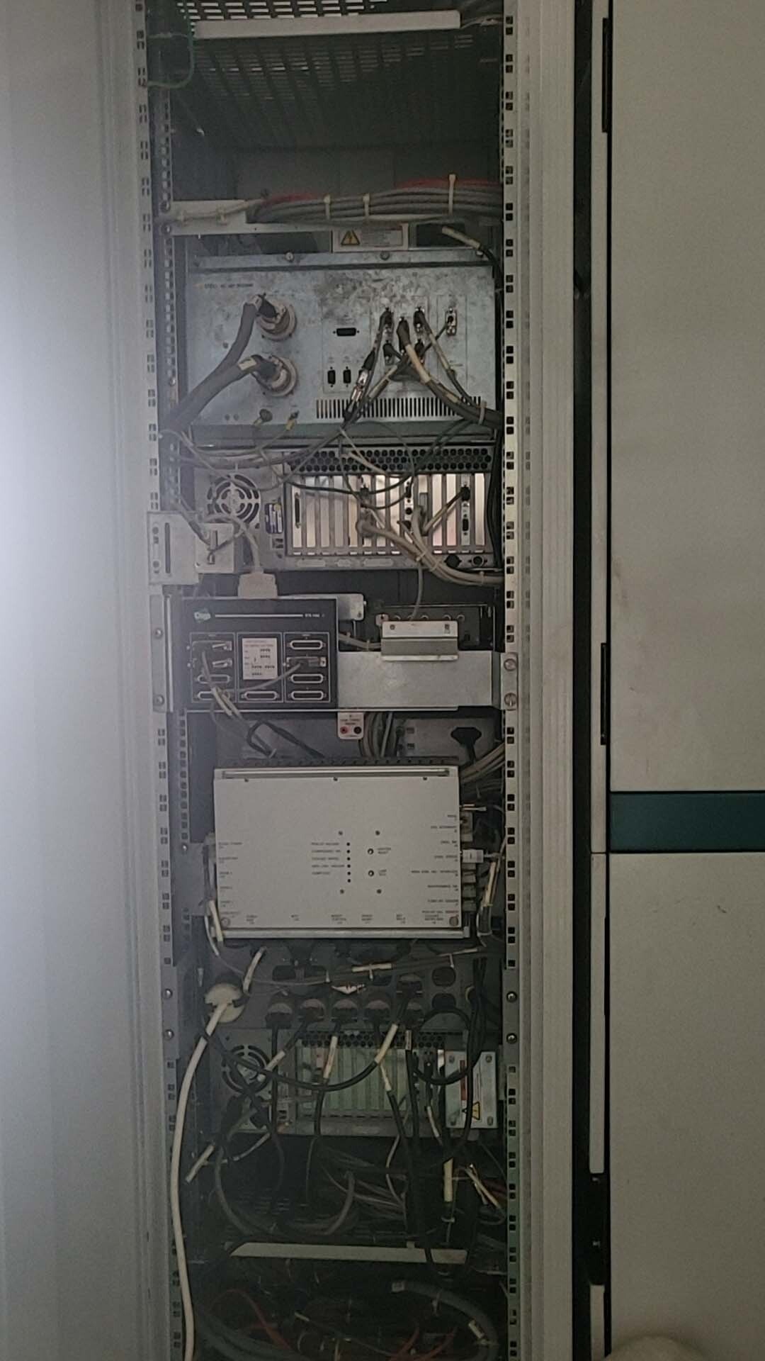

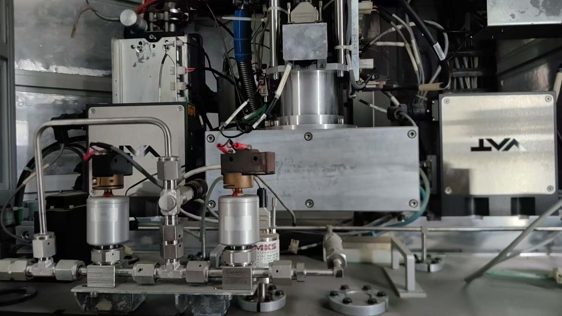
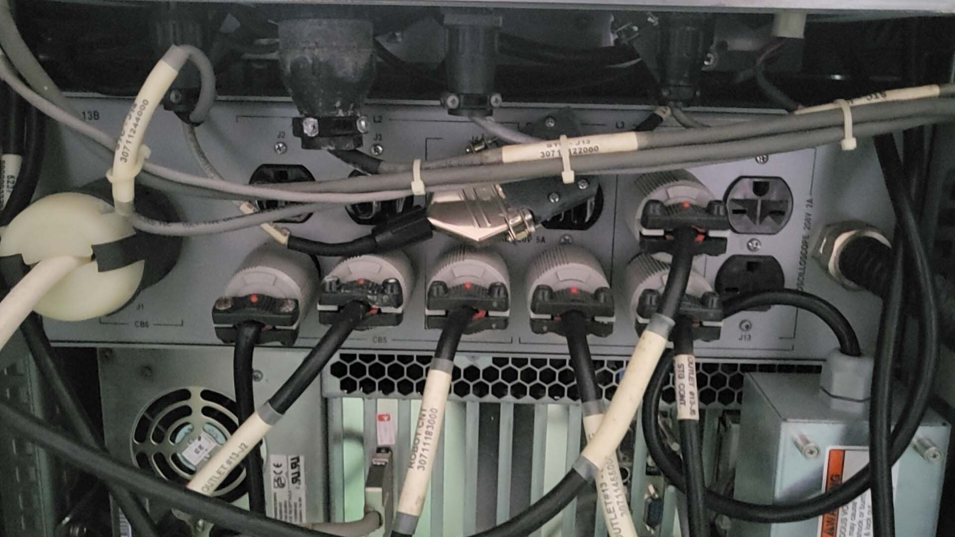
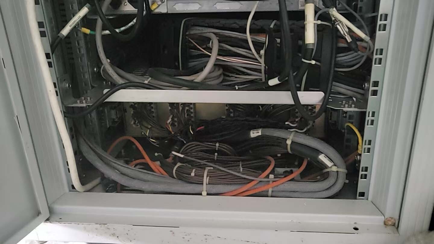
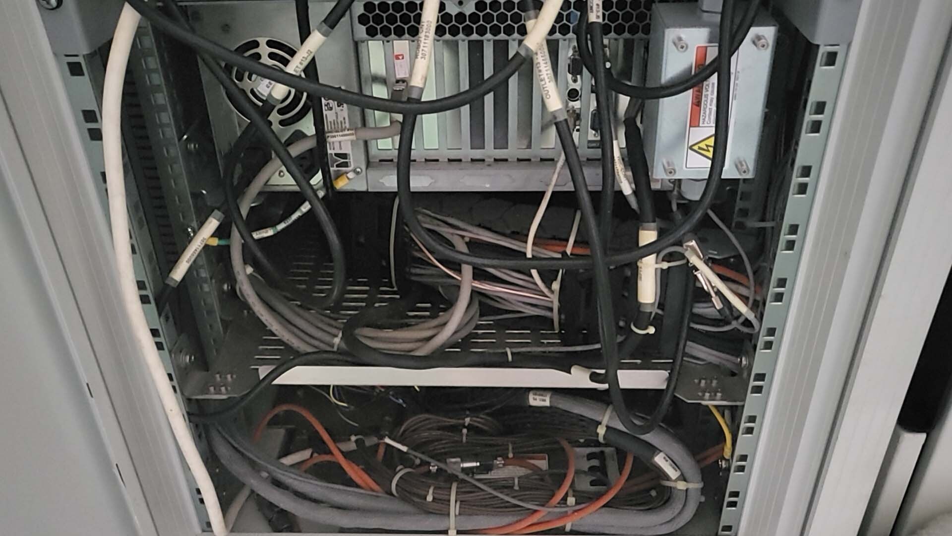
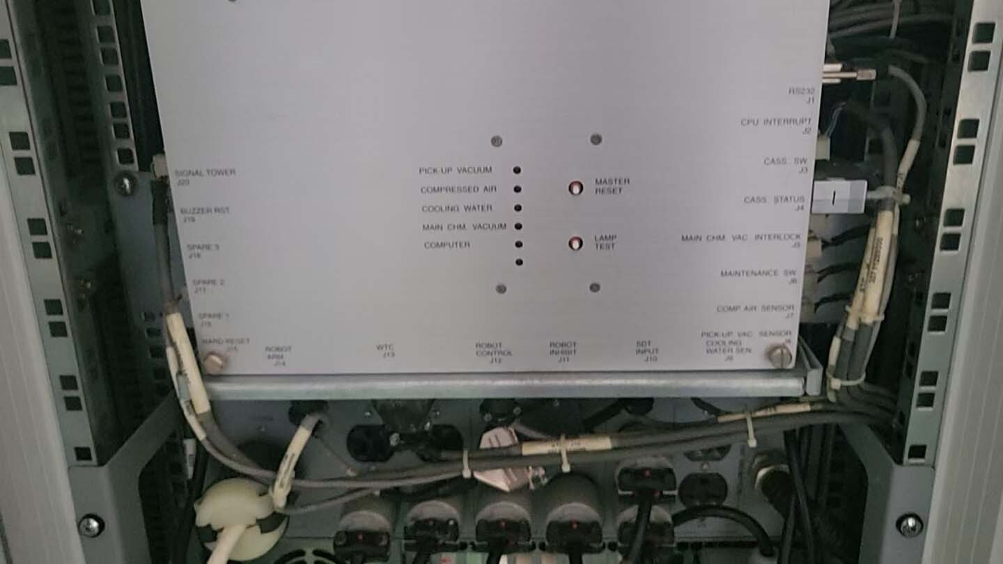
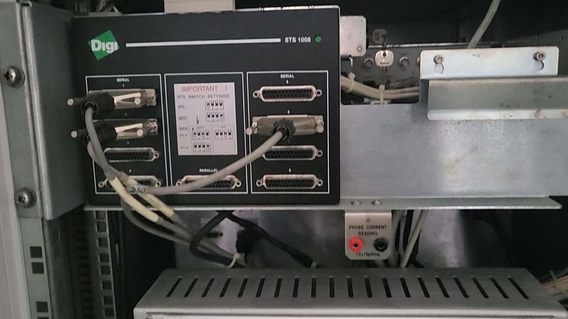
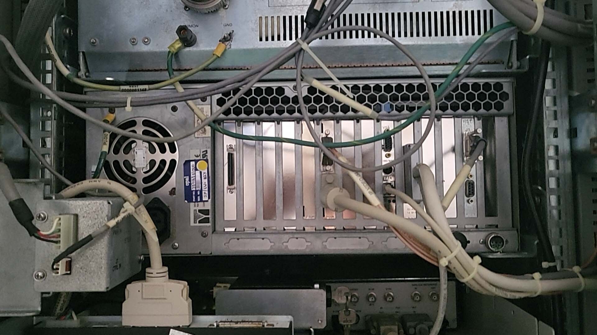
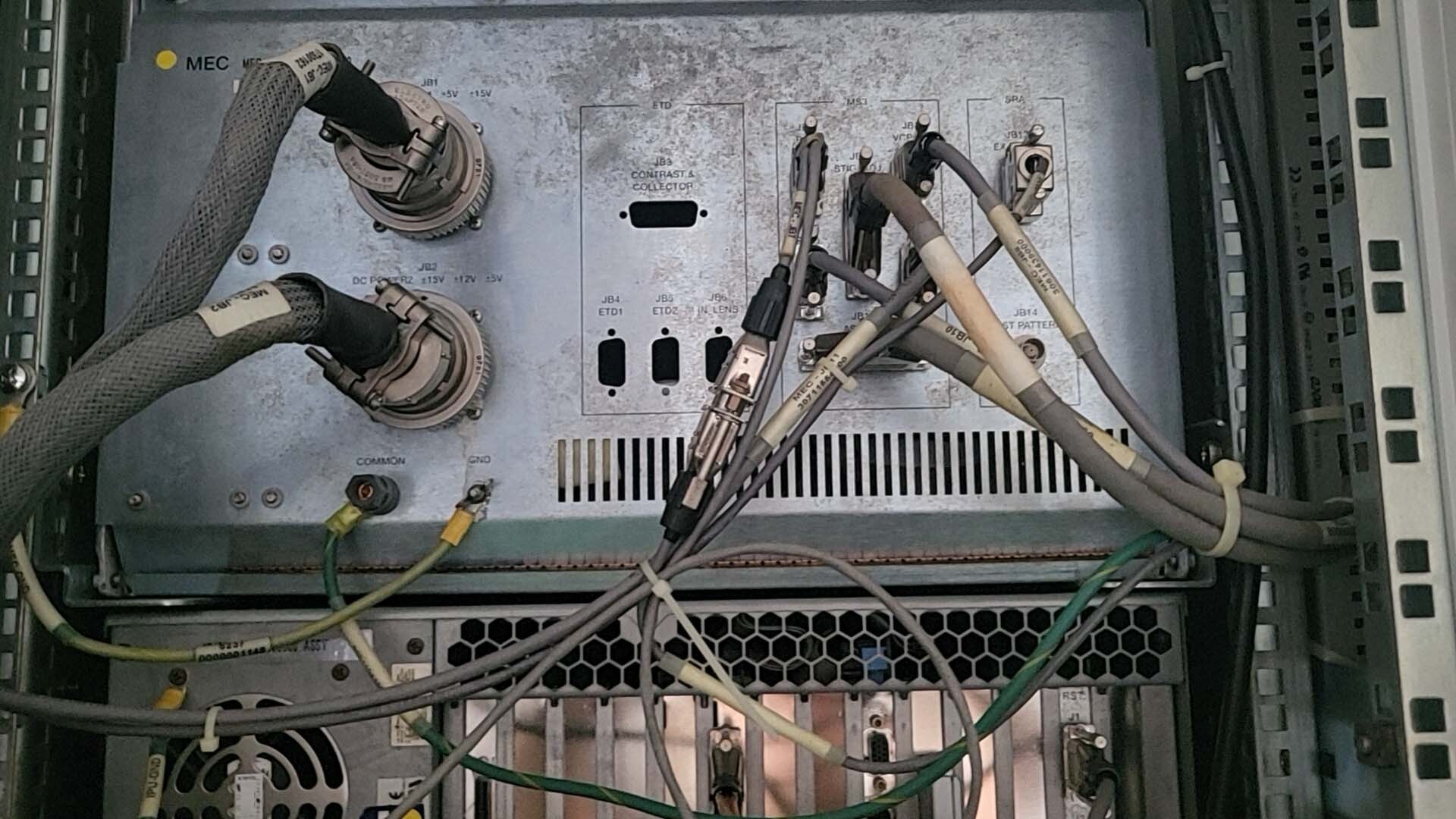
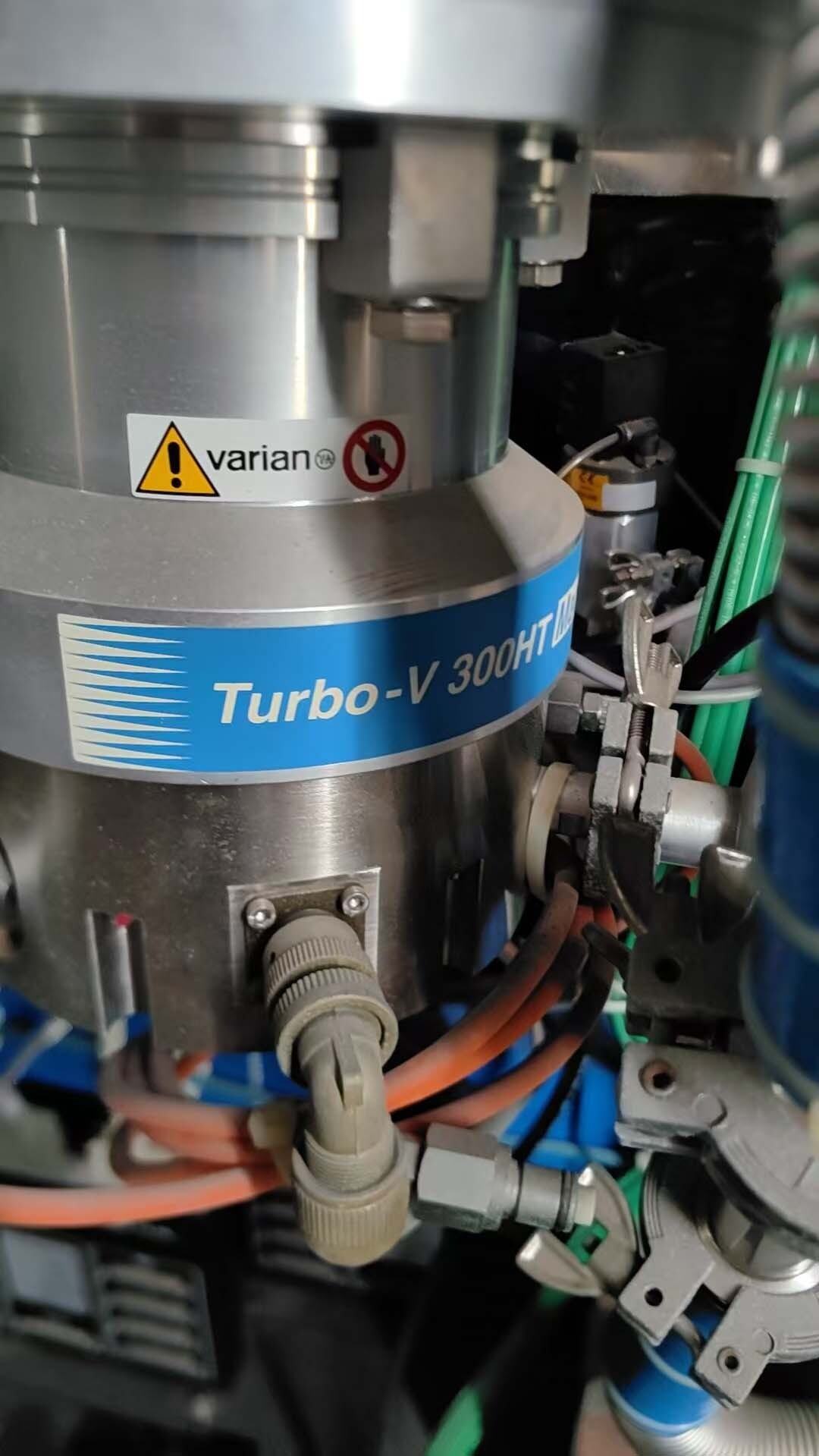
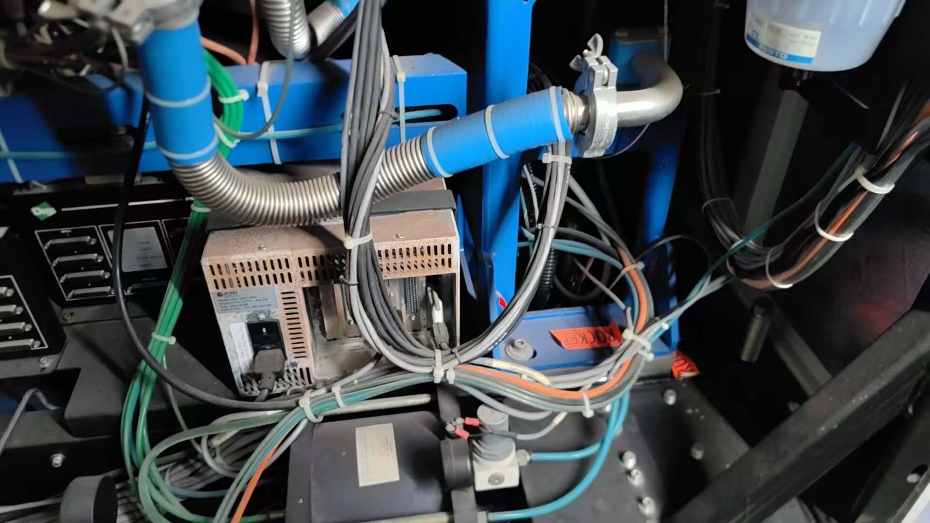
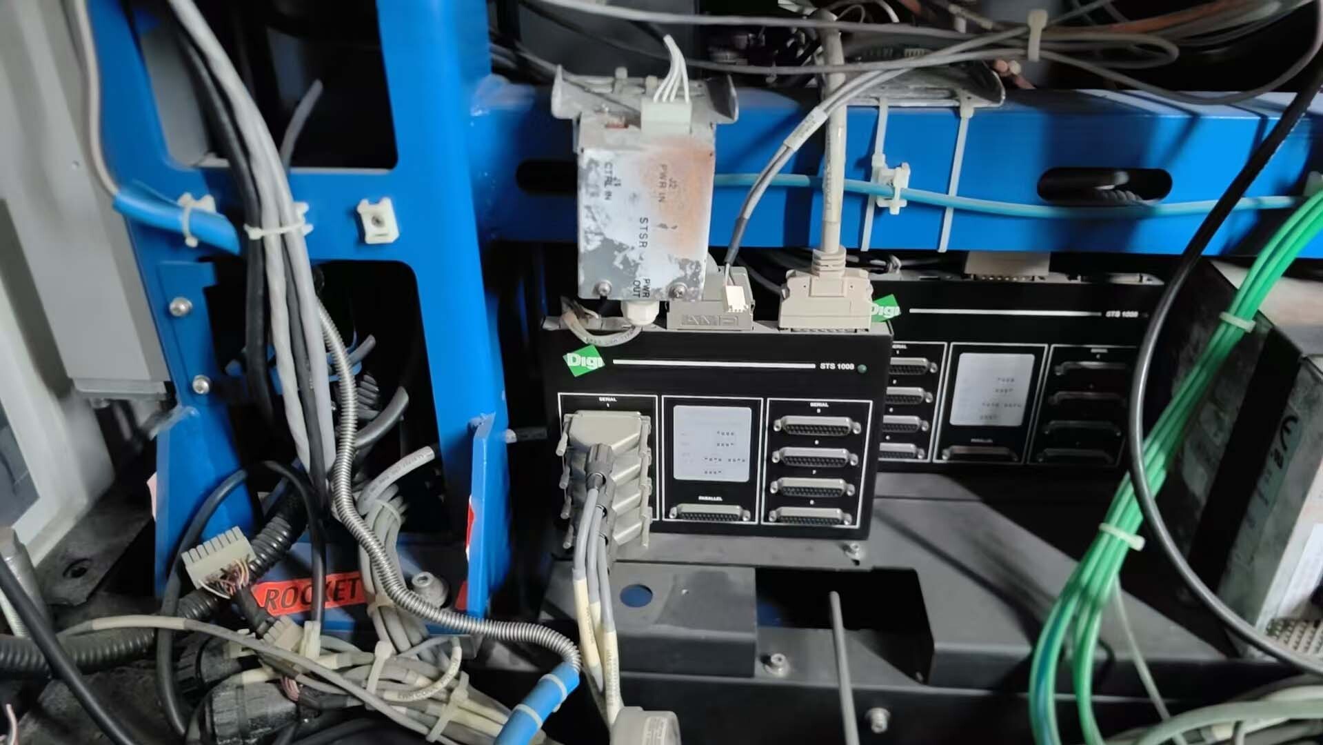
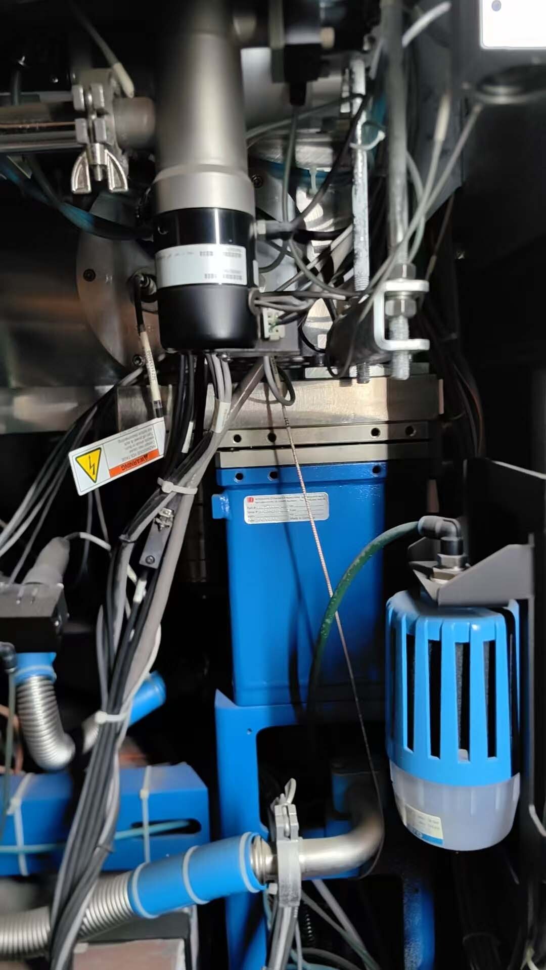
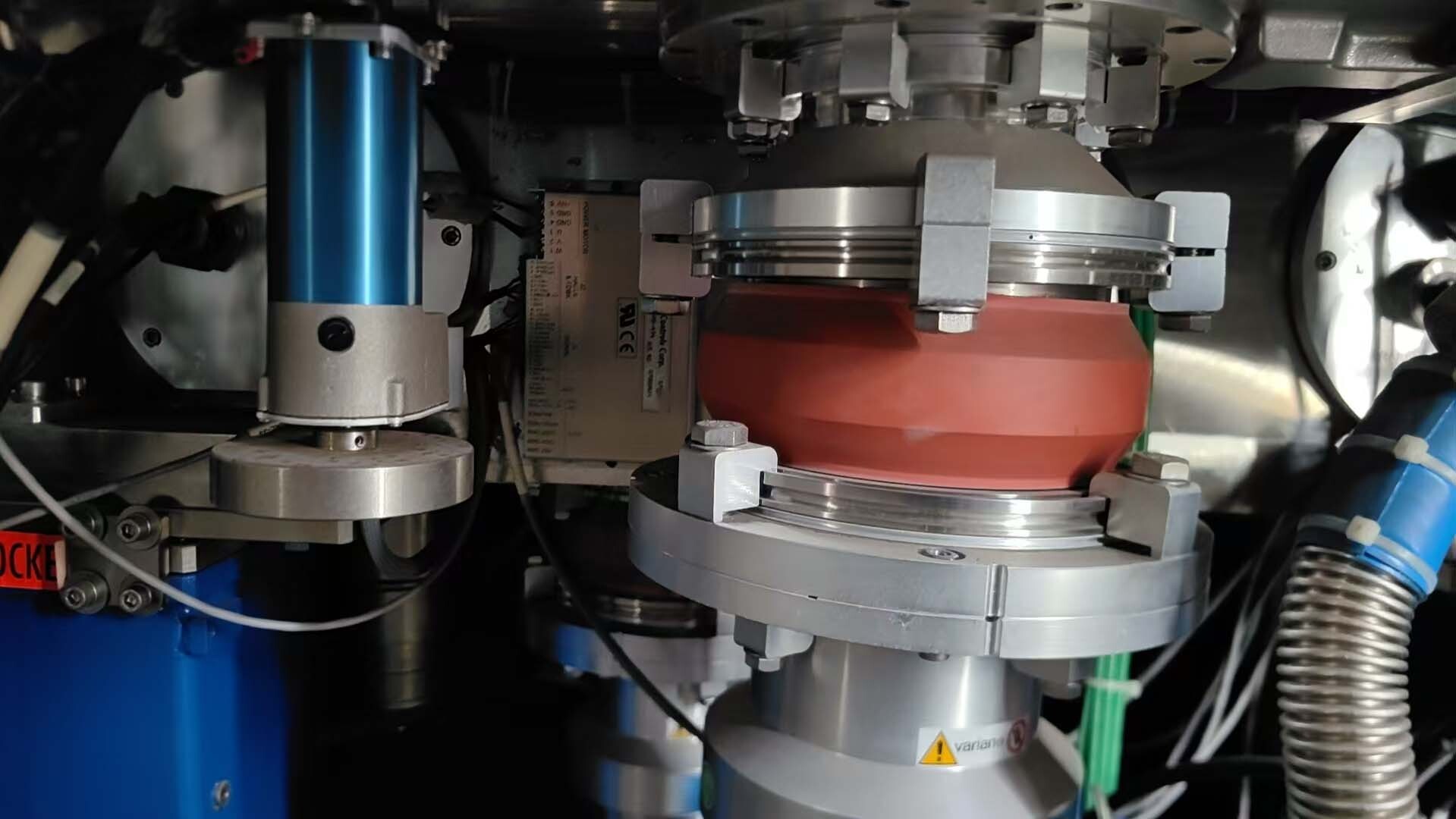
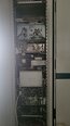
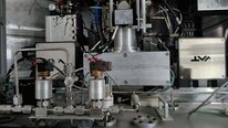
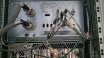
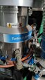
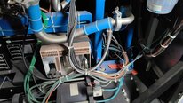
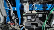
AMAT / APPLIED MATERIALS VeraSEM 3D Wafer Testing and Metrology Equipment is a high speed, high precision system that uses advanced algorithms to measure substrate morphology on a variety of semiconductor wafers. The unit quickly detects hazards and irregularities on the wafer surface, including particles, chips, scratches, and non-uniform deposits. The machine includes a series of automated analysis tools and image processing methods to rapidly characterize and analyze the morphology of the substrate. The hardware and optics of the VeraSEM tool are designed to rapidly acquire high-resolution SEM images and non-destructive test data of wafer structures. The automated analysis functions of the asset support automated defect analysis, surface roughness measurement, and multi-level metrology. It also includes a laser-based 3D measurement model to generate 3D map images that can be exported for further analysis. The equipment's algorithm-based defect detection and image analysis algorithms are designed to improve the accuracy and speed of defect and contamination detection. The algorithms use pattern recognition, segmentation, and shape recognition to accurately characterize the defect. The system can be programmed to perform a variety of analyses, from identifying particle size and location, to characterizing chips and scratches, to measuring non-uniform deposition. In addition to defect detection and analysis, AMAT VeraSEM 3D is also capable of measuring the morphological characteristics of the wafer substrate. It includes a number of functions to enable the measurement and analysis of surface, interface, and bulk properties of the substrate. It can measure surface topography, surface roughness, surface roughness of individual features, surface area, thickness variations, and other morphological features at multiple levels of detail. APPLIED MATERIALS VeraSEM 3D is an excellent tool to quickly and accurately characterize the surface morphology of substrate wafers. It can quickly detect a variety of hazards and irregularities on the wafer surface, and with its combination of automated image processing algorithms and 3D mapping capabilities, provide detailed analysis and visualization of the substrate structure.
There are no reviews yet