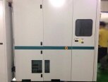
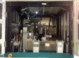
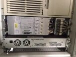
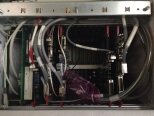
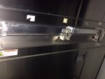
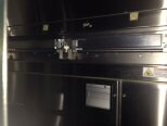
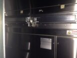
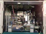
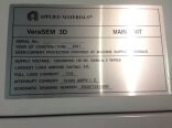
Used AMAT / APPLIED MATERIALS VeraSEM 3D #9123516 for sale
URL successfully copied!
Tap to zoom
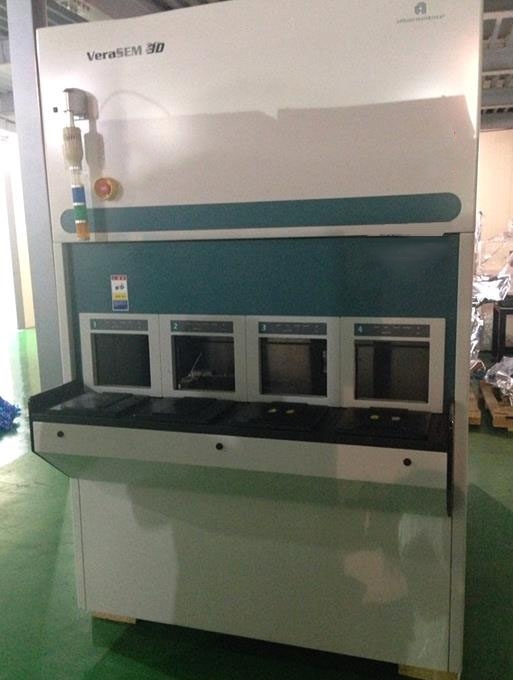

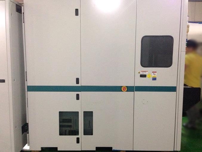

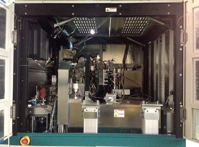

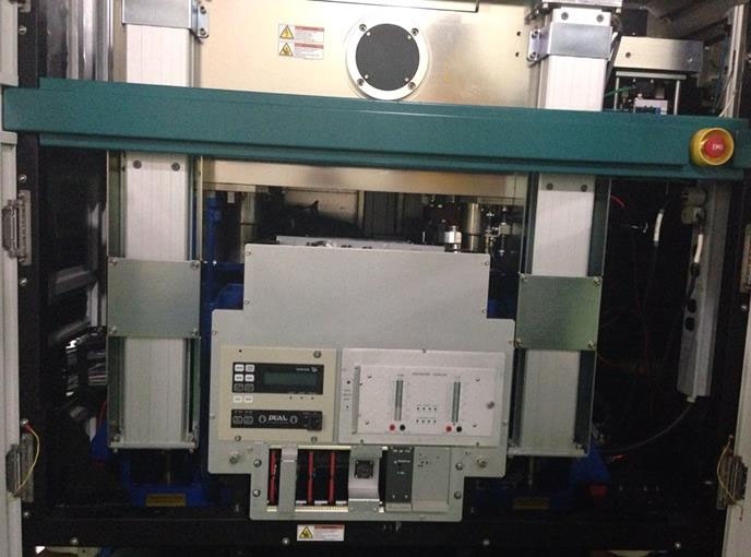

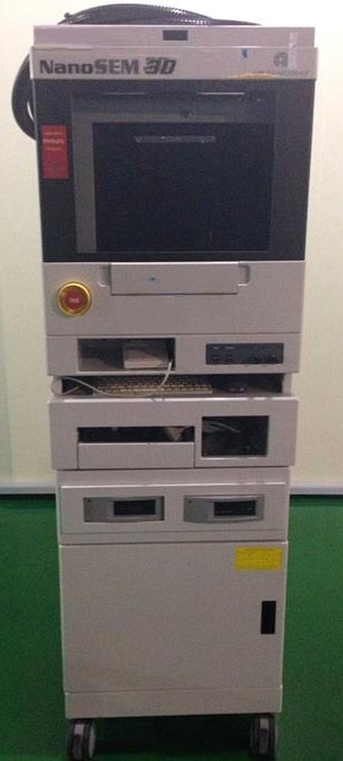

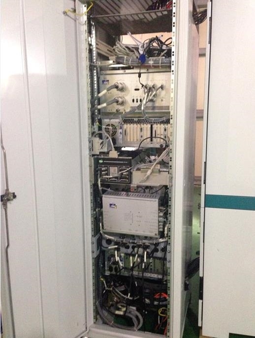

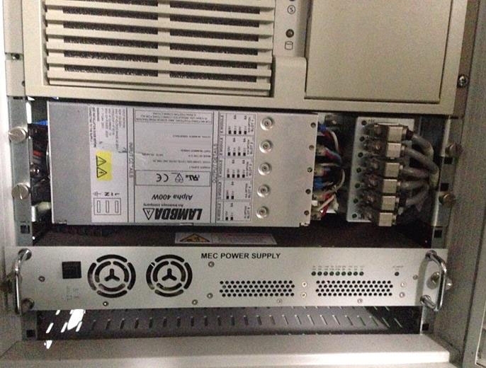

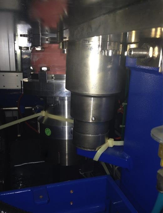

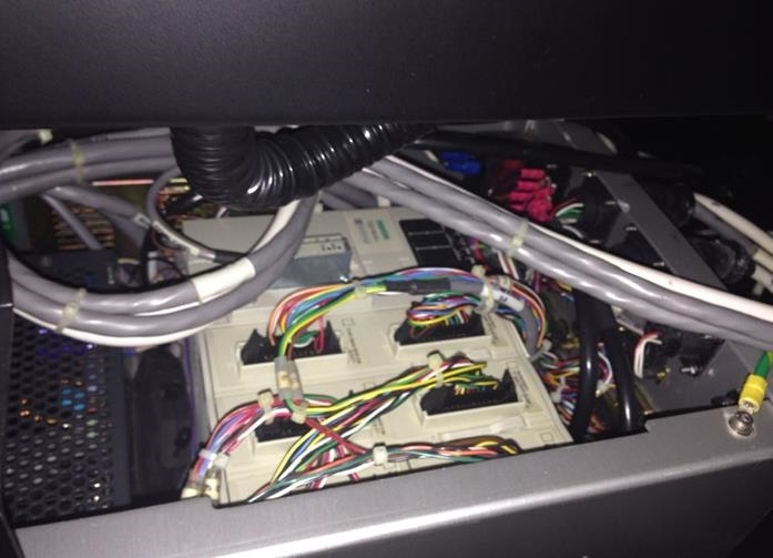

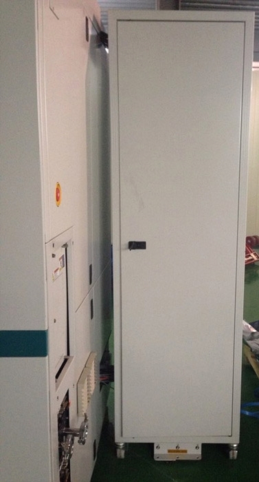

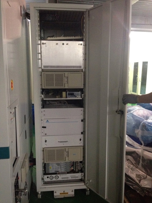

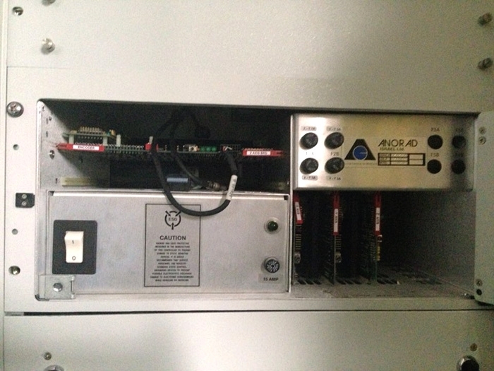

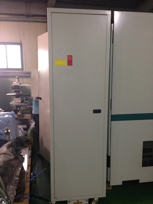


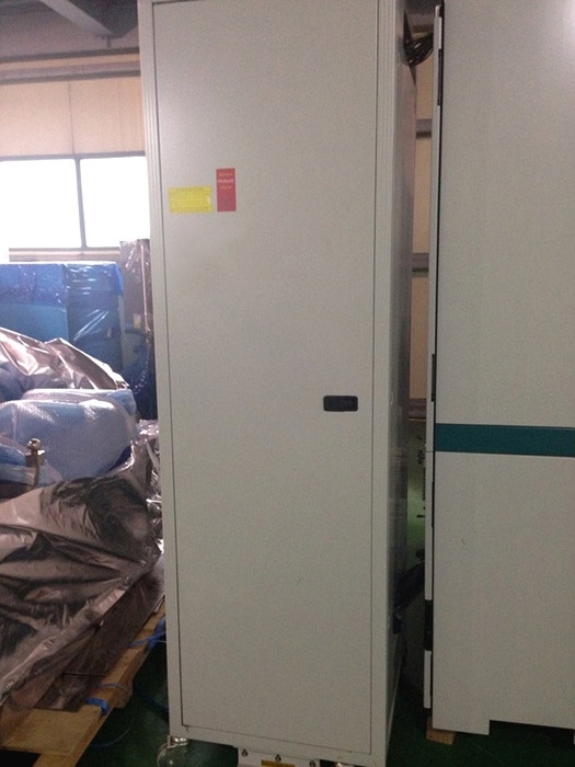


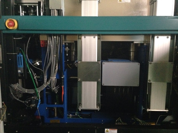

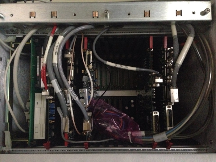

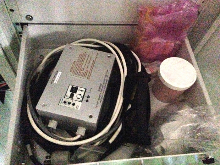


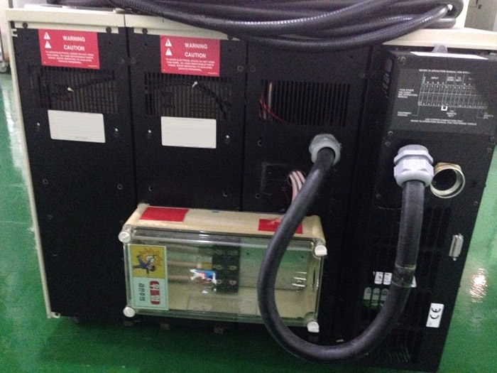






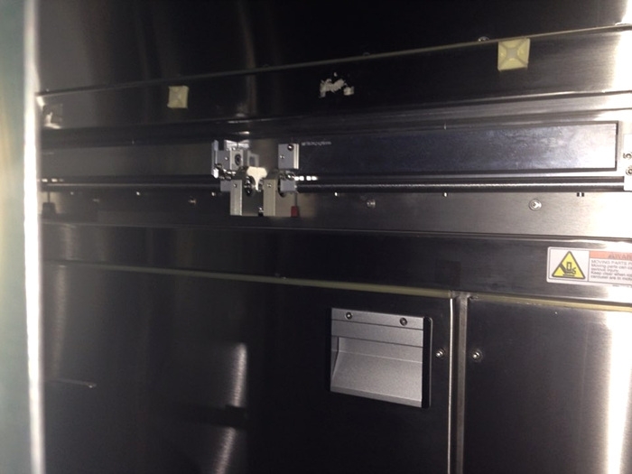

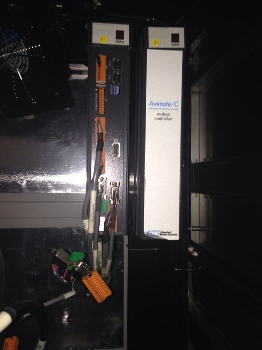


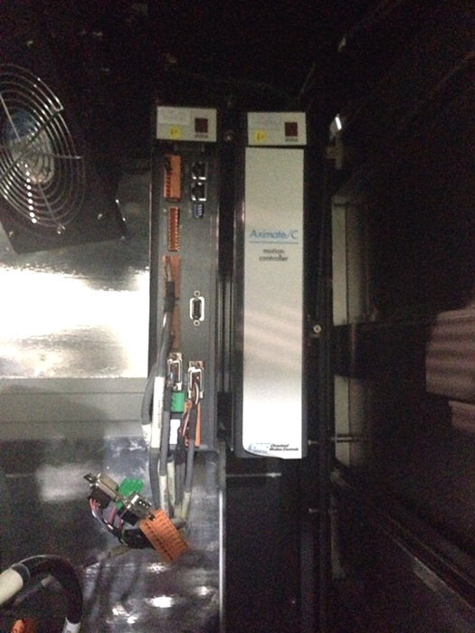

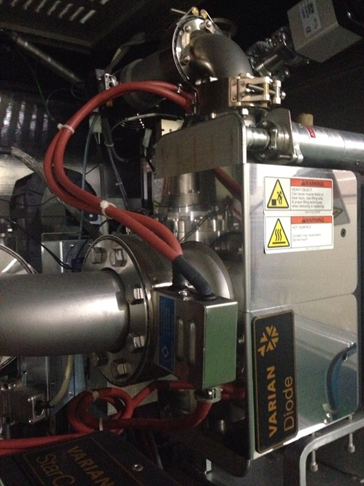

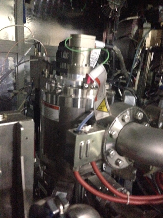

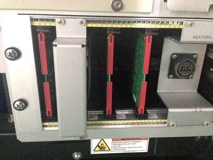

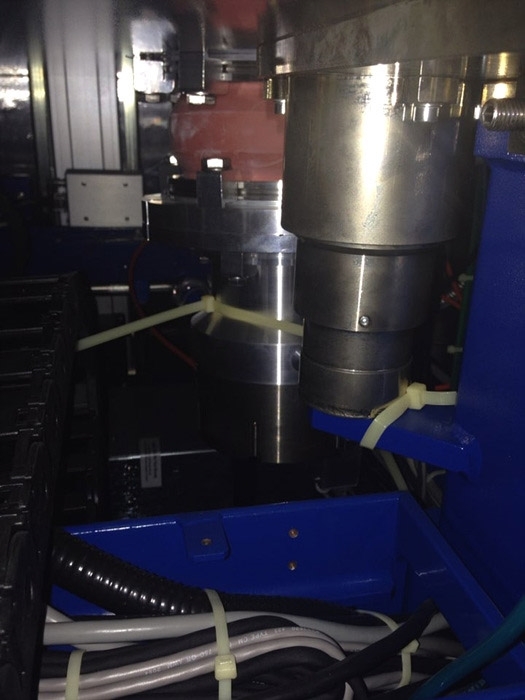





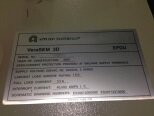
ID: 9123516
Wafer Size: 8"
Vintage: 2001
Automated CD metrology system, 8"
Wafer shape: SNNF (Semi Notch No Flat)
Wafer cassette: 8" PP (Miraial)
Electron optical system:
Electron gun SCHOTTKY emission source (FEI)
Accelerating voltage: 300 V - 2000 V
Prober current: Low 5pA / Medium 10pA / High 20pA
(3) Electromagnetic lenses
System with boosting voltage beam deflector module.
Objective lens:
Scan coil (2) stage electromagnetic deflection (X, Y)
Magnification: 1,000x to 400,000x (100 um to 0.25 um)
Aspect ratio: >14 : 1
Tilt function: 5° (4 Directions)
Resolution: 3 nm (500 V)
Optical microscope systems:
Camera monochrome with CCD camera
Magnification: 16x / 220x (450 um / 6000 um)
Wafer imaging ability entire surface, 8"
SECS / GEM Communication interface:
Automated image archiving function
Measurement function: Contact hole
Line edge analysis / CH Analysis / Slope
Measurement algorithm normal / Foot / Threshold
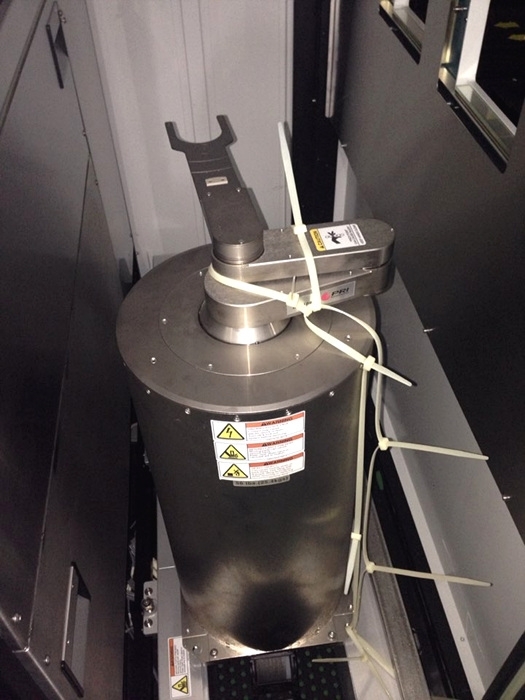
Wafer stage anorad X, Y and Z stage
Moving speed: 300 mm / sec
Function target faraday cup / Resolution target
Wafer shape ability notch / Orientation flat
Pre-alignment sensing CCD bar, 8"
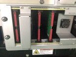
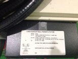
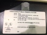
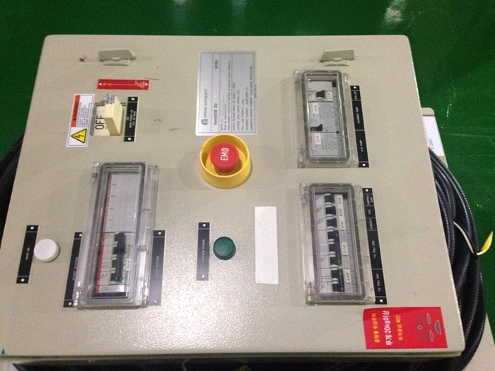
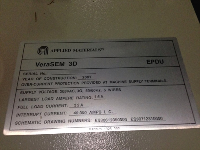
External power distribution unit
Fun filter unit
2001 vintage.
AMAT / APPLIED MATERIALS VeraSEM 3D is a state-of-the-art wafer testing and metrology equipment. It combines advanced optical microscopy techniques with metrology capabilities to provide highly accurate, non-destructive 3D characterization and analysis of semiconductor wafers. This powerful combination provides customers with accurate and repeatable characterization of wafers within the same chip and across multiple chips. AMAT VeraSEM 3D is designed to quickly measure and analyze nanoscale features of a semiconductor wafer with high precision and accuracy. The system utilizes a high-performance, sensitive CCD camera with a short wavelength range to acquire images of the surface of the wafer. This allows the user to accurately analyze the microscopic features and monitor their positions and dimensions. The images are stored and analyzed in a specialized software package that can detect and measure overlays, CDs, linewidths, vias, pits and other features. APPLIED MATERIALS VeraSEM 3D also includes an integrated metrology unit to help accurately measure wafer surface features such as flatness, roughness and shape. This machine uses advanced algorithms and computer-controlled laser scanning to measure a wide range of features including line-widths, pitches, surface steps and gaps of semiconductor devices. The tool also supports advanced pattern recognition algorithms that can locate and analyze defects on the surface of the wafer even in challenging environments. This allows users to quickly detect and quantify wafer defects with high accuracy, improving the reliability and quality of semiconductor devices. The combination of powerful microscopy and metrology capabilities of VeraSEM 3D make it an ideal solution for wafer fabrication and monitoring. The asset's performance is comparable to electron microscopes but it is much faster and easier to use, making it highly attractive for customers in the semiconductor industry.
There are no reviews yet

