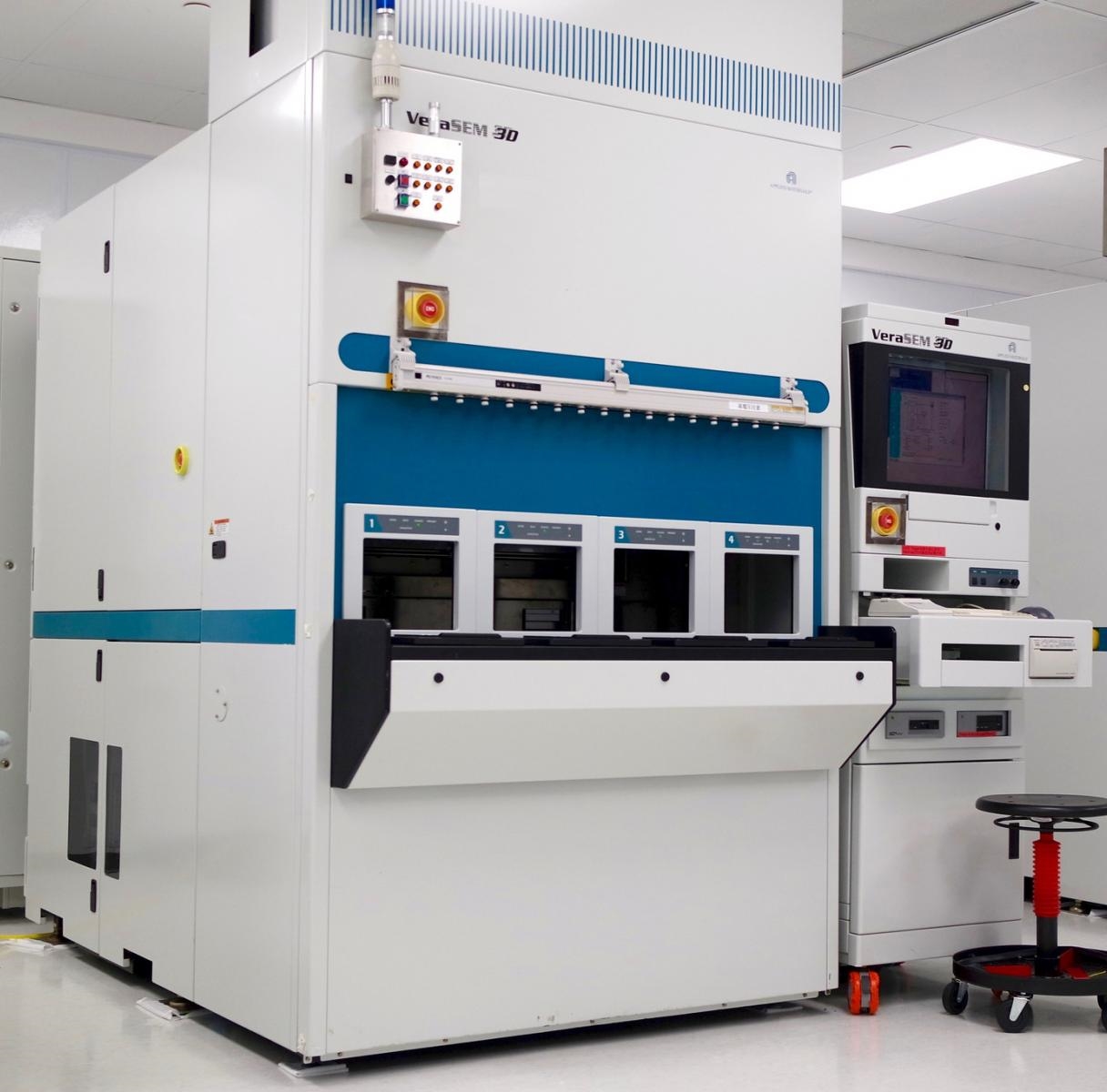
Used AMAT / APPLIED MATERIALS VeraSEM 3D #9138846 for sale
It looks like this item has already been sold. Check similar products below or contact us and our experienced team will find it for you.
Tap to zoom


Sold
ID: 9138846
Wafer Size: 8"
Vintage: 2001
Automated CD metrology system, 8"
Open cassette
Wafer shape: Semi notch no flat (SNNF)
Wafer cassette: PP Miraial, 8"
Objective lens:
Scan coil 2-stage electromagnetic deflection (X- and Y-Axes)
Magnification: 1,000x to 400,000x (100um to 0.25um FOV)
Wafer imaging ability entire surface, 8"
Aspect ratio >14 : 1
Tilt function 5 degrees (4 Direction)
Resolution: 3nm (500V)
Optical microscope system:
Camera monochrome: CCD Camera
Magnification: 16x / 220 x (450 um / 6000 um FOV)
Wafer imaging ability entire surface, 8"
Wafer stage:
Wafer stage Anorad XY and Z Stage
Moving speed: 300 mm/sec
Function target faraday cup / Resolution target
Wafer transfer:
Wafer shape ability notch / Orientation flat
Pre-alignment sensing by CCD BAR (8")
External power distribution unit
Fun filter unit
Electron optical system:
Electron gun SCHOTTKY Emission source (FEI)
Accelerating voltage: 300V to 2,000V
Electromagnetic lens 3 stage electromagnetic lens
System with boosting voltage beam deflector module
Probe current:
Low: 5 pA
Medium: 10 pA
High: 20 pA
2001 vintage.
AMAT / APPLIED MATERIALS VeraSEM 3D is an advanced wafer testing and metrology equipment. This system enables precision analysis of a range of wafer production processes, including deposition, etching, lithography, and mask processing. AMAT VeraSEM 3D offers a range of powerful instruments, including electron microscopy and autonomous optical microscopy. APPLIED MATERIALS VeraSEM 3D is a high-performance unit offering a host of features and benefits to meet the needs of both production and research and development environments. The principal tool used in the machine is the electron microscope, which enables the user to measure the features of a wafer accurately and prepare a complete topographical map of the sample. This map can be used to detect defects, substructure, and composition of deposited layers. The microscope also enables in-depth analysis of the internal structure of the wafer, with measurements of over 50 surface parameters available. Other features of the electron microscope include automated particle analysis and advanced imaging capabilities. The secondary instrument used in VeraSEM 3D is an autonomous optical microscope, which utilizes a range of optical technologies to accurately measure the depth and feature sizes of surface structure. This tool is highly versatile and is capable of measuring a wide range of feature dimensions on a range of wafer substrates. The microscope is also able to measure the distribution of different types of contaminants present on the wafer surface. AMAT / APPLIED MATERIALS VeraSEM 3D asset also incorporates a range of advanced data acquisition and analysis tools. These tools allow for accurate automation of the processes involved in wafer testing and metrology. This model can also be interfaced with other systems or software, allowing users to access a wealth of data from a variety of sources. AMAT VeraSEM 3D is an industry-leading equipment which allows users to accurately test and measure many aspects of wafer production. Its range of features and powerful instruments ensure that this system is a valuable asset to any research and development or production environment.
There are no reviews yet