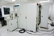
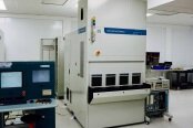
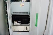
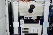
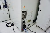
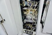
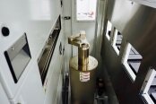
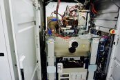
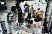
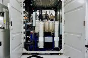
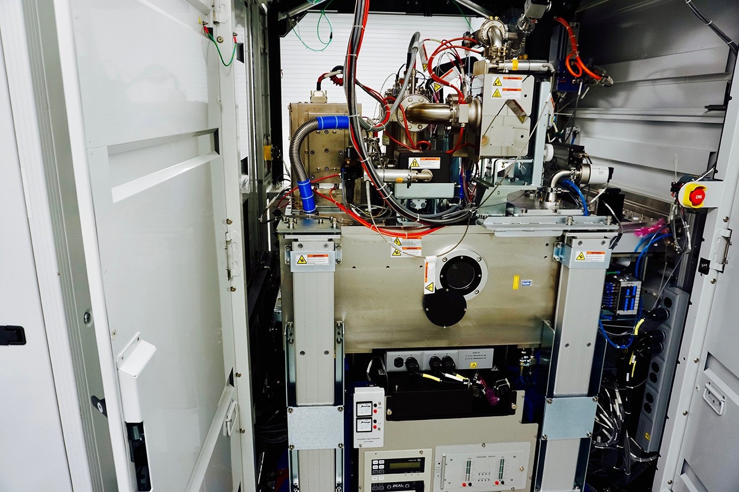
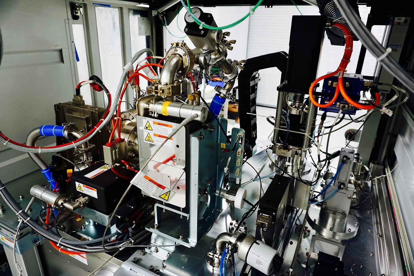
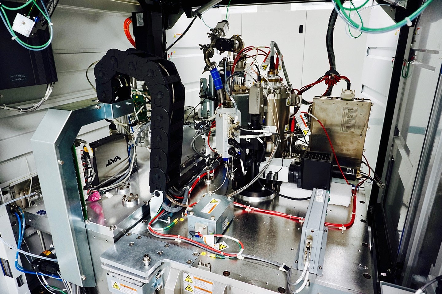
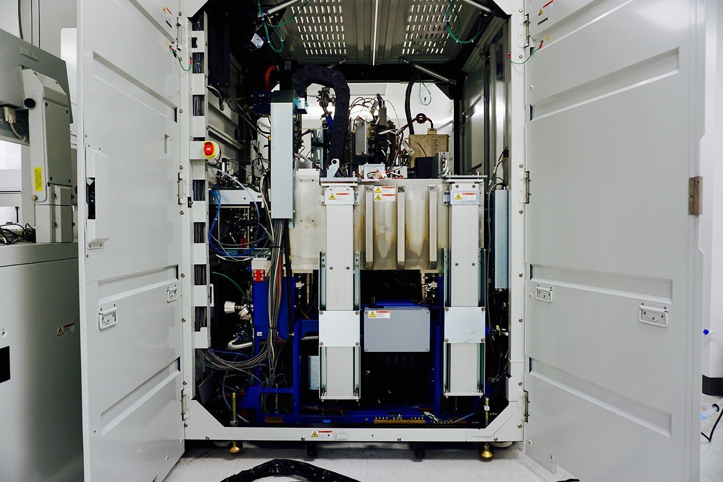
Used AMAT / APPLIED MATERIALS VeritySEM #9280532 for sale
URL successfully copied!
Tap to zoom
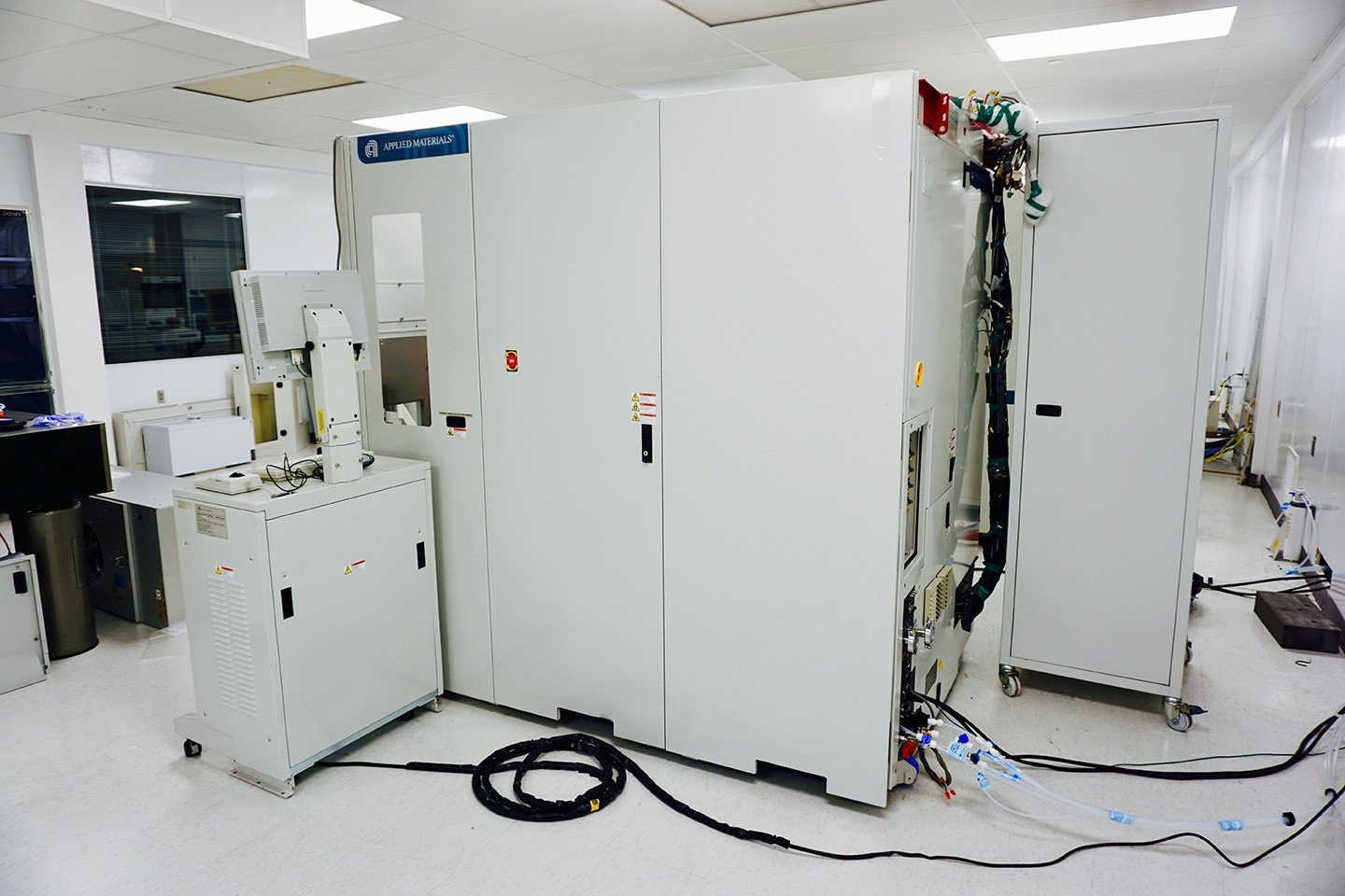

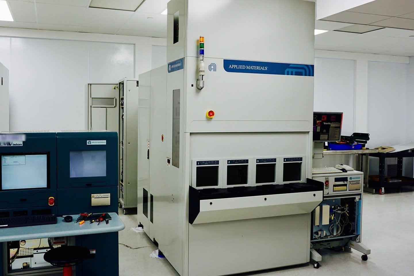


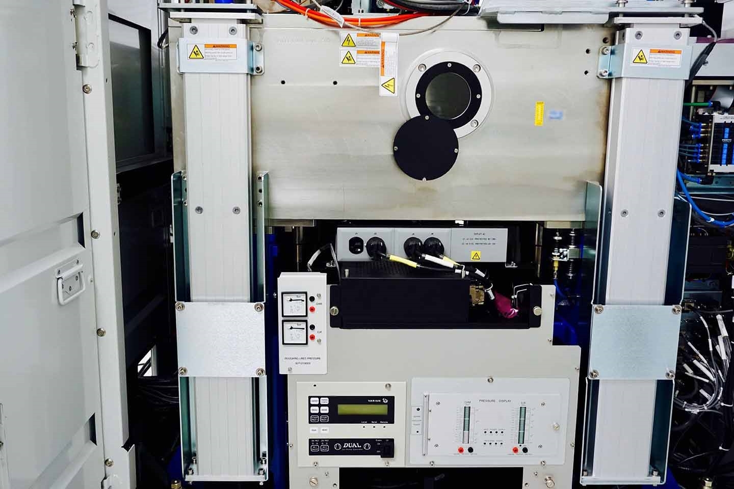

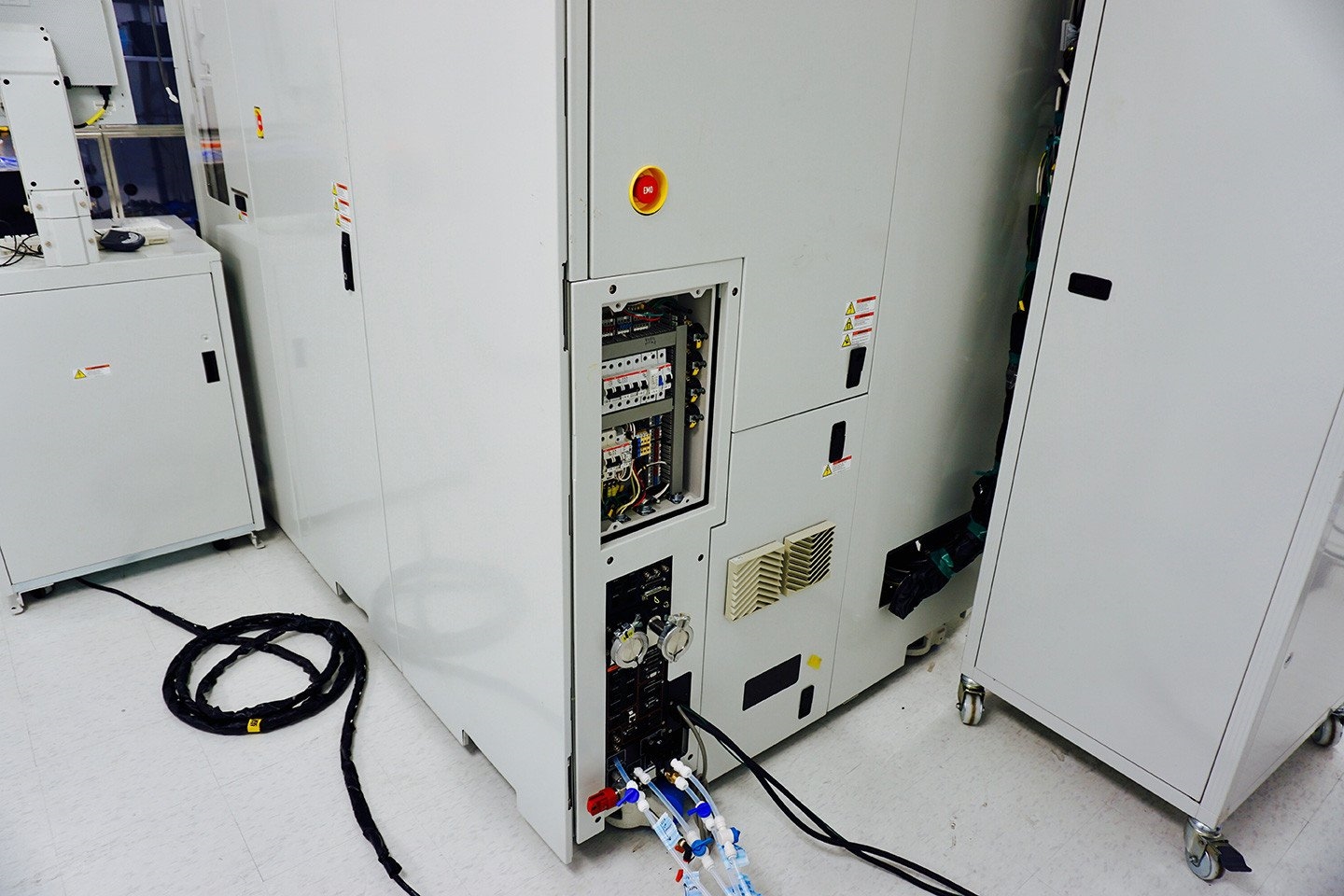

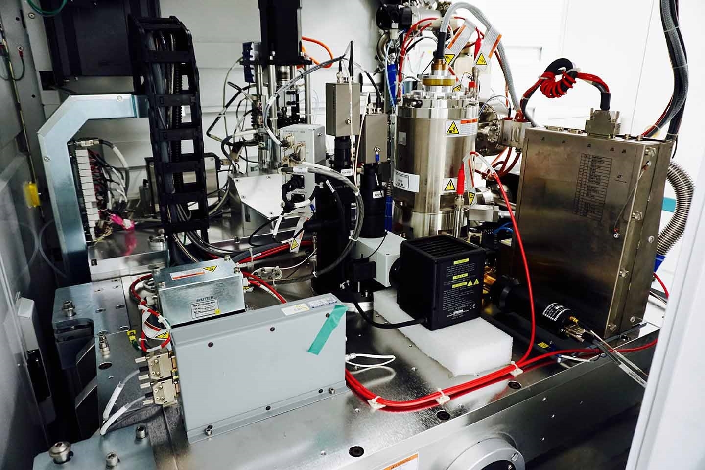

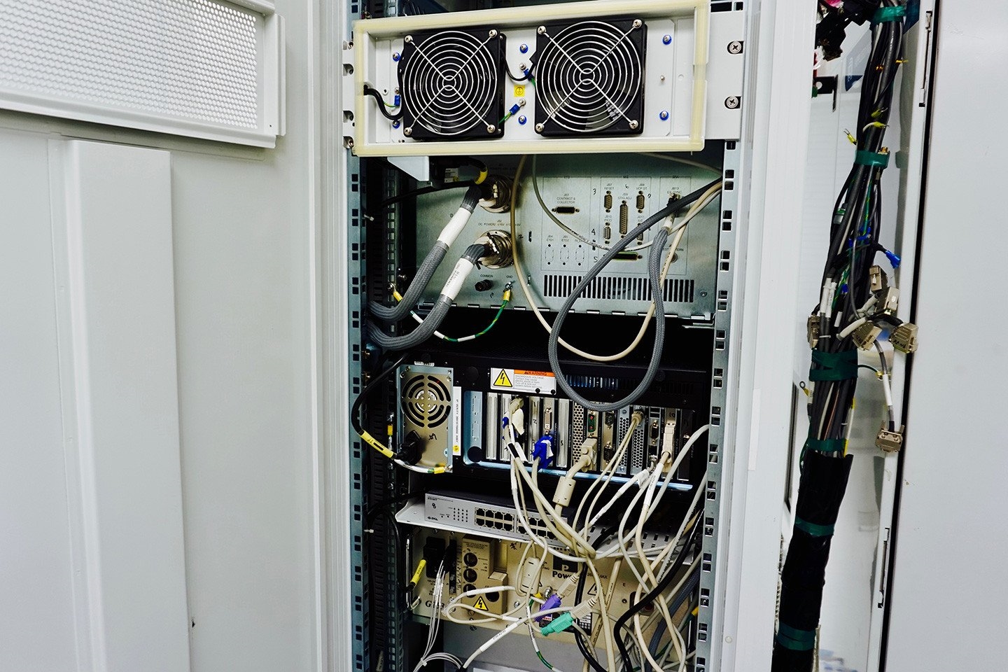

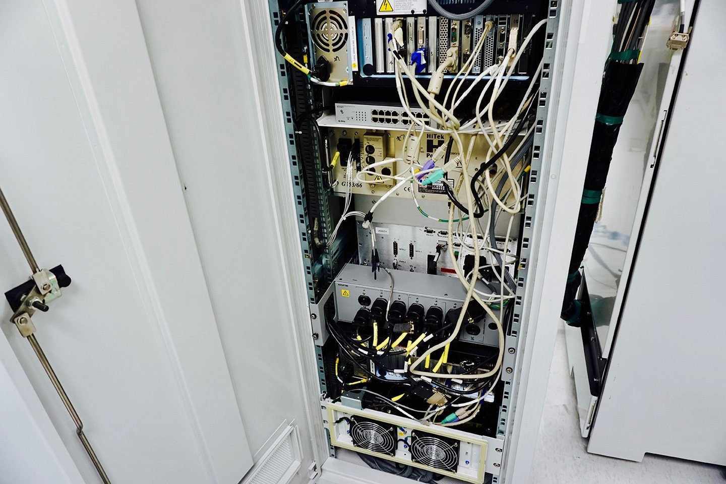

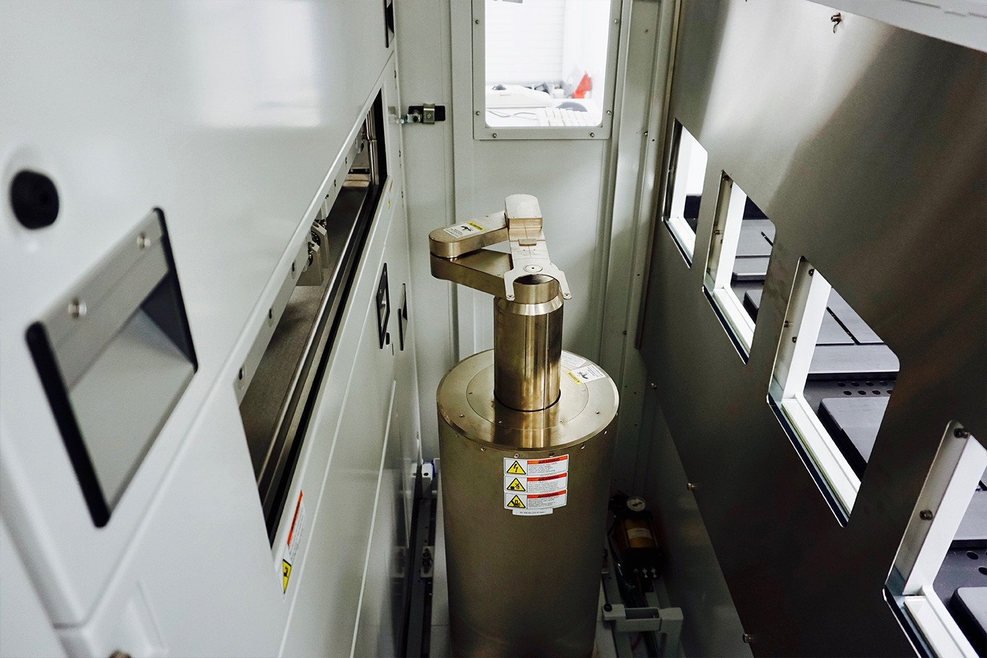

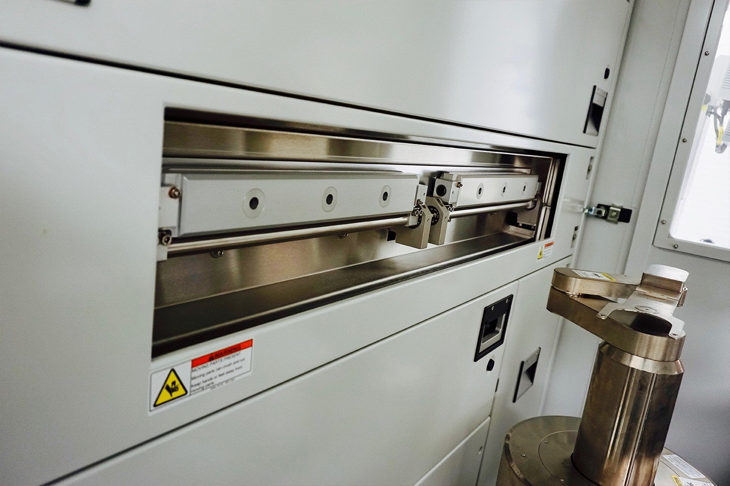

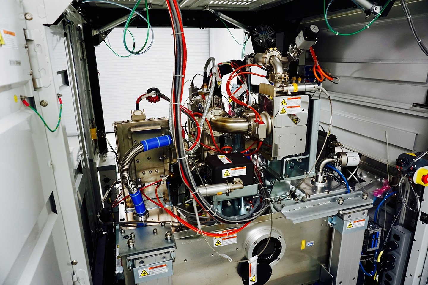





ID: 9280532
Wafer Size: 8"
Automated CD metrology system, 8"
Wafer shape: SNNF (Semi Notch No Flat)
Wafer cassette: PP Miraial, 12"
No SMIF Interface
Electron optical system:
Electron gun SCHOTTKY emission source (FEI)
Accelerating voltage: 300 V - 2000 V
Prober current: Low 5pA / Medium 10pA / High 20pA
3-Stage Electromagnetic lenses
System with boosting voltage beam deflector module
Objective lens:
Scan coil 2-stages: Electromagnetic deflection (X-axis & Y-axis)
Magnification: 1,000x - 400,000x (100um - 0.25um FOV)
Wafer imaging ability entire surface, 8"
Aspect ratio: >20:1
Resolution: 2nm (500V)
Optical microscope system:
Camera monochrome: CCD Camera
Magnification: 16x / 220x (450 um / 6000 um FOV)
Wafer imaging ability entire surface, 12"
Model SGI Fuel
SECS / GEM Communication interface:
Automated image archiving function / Online setup
Measurement function: Contact hole
Line edge analysis / CH Analysis / Slope
Measurement algorithm normal / Foot / Threshold
Wafer stage:
Wafer stage Anorad XY and Z Stage
Moving speed: 300 mm/sec
Function target faraday cup / Resolution target
Wafer transfer:
Wafer shape ability notch / Orientation flat
Pre-alignment sensing by CCD BAR (200/300 mm wafer)
External power distribution unit
Fun filter unit.
AMAT / APPLIED MATERIALS VeritySEM is a scanning electron microscope (SEM) that offers superior imaging capabilities and precision control for advanced failure analysis and process development in the semiconductor industry. This versatile equipment gives users a complete range of advanced capabilities, from high-resolution imaging to spectroscopic analysis, while providing a stable and reliable platform for consistent, accurate imaging results. AMAT VeritySEM is a variable pressure SEM system, offering both ultra-high vacuum and low vacuum imaging capabilities. Its low-vacuum mode enables surface imaging and analysis over a wide range of pressures from 0.1-50 torr, including full-range imaging under an inert gas to prevent specimen charging. The unit also features a fast vacuum valve control technology, ensuring quick and reliable purging and conditioning of the specimen chamber. This vacuum technology combined with precise control over the imaging mode and conditions allows the user to get consistent, accurate imaging results for hard-to-image specimens. In addition to its advanced imaging capabilities, APPLIED MATERIALS VeritySEM also offers advanced spectroscopy capabilities. Its efficient, automated sample handling and high secondary electron yield combine with a wide range of spectroscopic analysis tools for superior resolution and contrast in individual components and in small feature sizes for nanoscale imaging. VeritySEM supports a variety of analytical techniques such as EDX, WDX, SEI spectroscopy, and CL analysis. AMAT / APPLIED MATERIALS VeritySEM comes with an integrated spot-analysis control module which provides fast, automated sample handling and positioning, as well as proven stability for significantly improved signal-to-noise ratios for challenging samples. The integrated image analysis machine (IAS) features powerful contrast control and measurement ability, along with high-resolution imaging and low noise, and offers unparalleled finesse imaging of otherwise difficult samples. AMAT VeritySEM is designed to enable fast turnaround of analysis results, and its advanced features such as automated specimen positioning, integrated spot analysis, highly detailed image analysis, and automated standards validation ensure reliable and fast results from a wide variety of samples. It is a reliable tool for advanced failure analysis and process development in the semiconductor industry and offers a uniquely powerful set of features at an extremely competitive price.
There are no reviews yet
