Used AMBIOS TECHNOLOGY XP-1 #293826375 for sale
URL successfully copied!
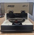
Tap to zoom
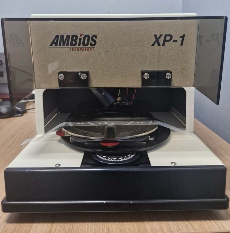

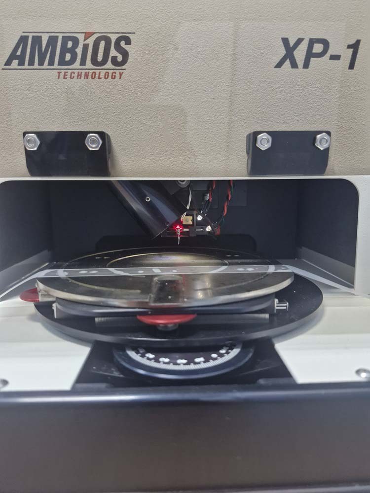
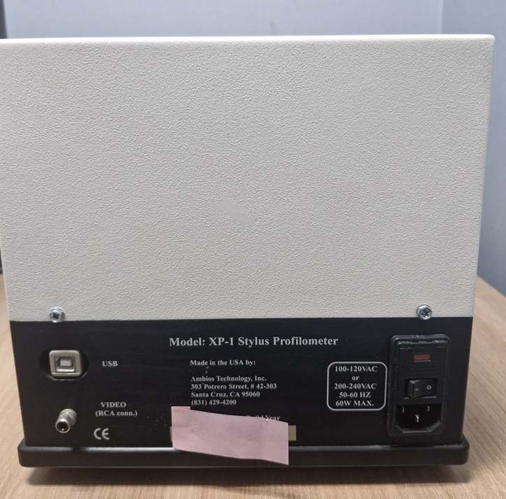
ID: 293826375
Surface profilometer
Sample stage diameter: 140mm
Scan length range: 30mm Maximum
Sample thickness: 20mm Maximum
Vertical resolution: 1.0Å at 10µm
Vertical range: 400µm max
Step height repeatability: 6Å on 1µm Step
Max. data points per scan: 120000
Sample viewing: Color camera
Magnification: 100x Fixed
Stylus tip radius: 2.0 Micron
Stylus force range: 0.05-10mg (Programmable).
AMBIOS TECHNOLOGY XP-1 is a cutting-edge wafer testing and metrology equipment designed for high-precision surface measurement and analysis in semiconductor manufacturing and research environments. This advanced instrument offers a wide range of capabilities for characterizing wafer surfaces with unmatched accuracy and efficiency, making it an indispensable tool for ensuring the quality and performance of semiconductor devices. At the core of XP-1 system is its innovative interferometric technology, which enables non-contact, high-resolution surface profiling with sub-nanometer precision. This technology utilizes laser interferometry to precisely measure the height variations of a wafer surface, providing detailed information about surface roughness, morphology, and defects at the nanoscale level. By capturing interferometric data, AMBIOS TECHNOLOGY XP-1 can generate 3D topography maps of wafer surfaces with exceptional spatial resolution, allowing users to visualize and analyze surface features with unparalleled detail. XP-1 unit is equipped with a state-of-the-art XYZ scanning stage that enables automated, programmable movement of the wafer under the measurement head. This stage provides precise control over the positioning and scanning speed, allowing users to capture surface data over large areas or specific regions of interest with high throughput and repeatability. The machine's advanced control software offers a user-friendly interface for setting up measurement routines, defining scan parameters, and visualizing real-time data feedback during the measurement process. In addition to surface profiling, AMBIOS TECHNOLOGY XP-1 tool offers a range of metrology capabilities for analyzing various surface properties of semiconductor wafers. The asset can perform measurements of surface roughness, step height, line width, and other critical parameters with exceptional accuracy, making it suitable for quality control, process monitoring, and failure analysis applications in semiconductor fabrication facilities. The model's comprehensive data analysis tools enable users to extract valuable insights from the measured data, such as statistical distributions, trend analysis, and correlation studies, to optimize manufacturing processes and enhance product performance. XP-1 equipment is designed to be versatile and adaptable to different wafer sizes, materials, and surface conditions commonly encountered in semiconductor manufacturing. The system's modular design allows for easy integration of additional measurement modules, such as optical profilometry, atomic force microscopy, or confocal microscopy, to expand its measurement capabilities and versatility. The unit can be customized with a range of options, including automated wafer handling, environmental control chambers, and advanced data processing algorithms, to meet the specific requirements of different semiconductor applications. Overall, AMBIOS TECHNOLOGY XP-1 wafer testing and metrology machine offers a comprehensive solution for high-precision surface characterization in semiconductor manufacturing and research settings. With its advanced interferometric technology, automated scanning capabilities, and versatile measurement modules, XP-1 tool provides reliable, accurate, and efficient surface analysis for ensuring the quality and reliability of semiconductor devices in the ever-evolving semiconductor industry.
There are no reviews yet