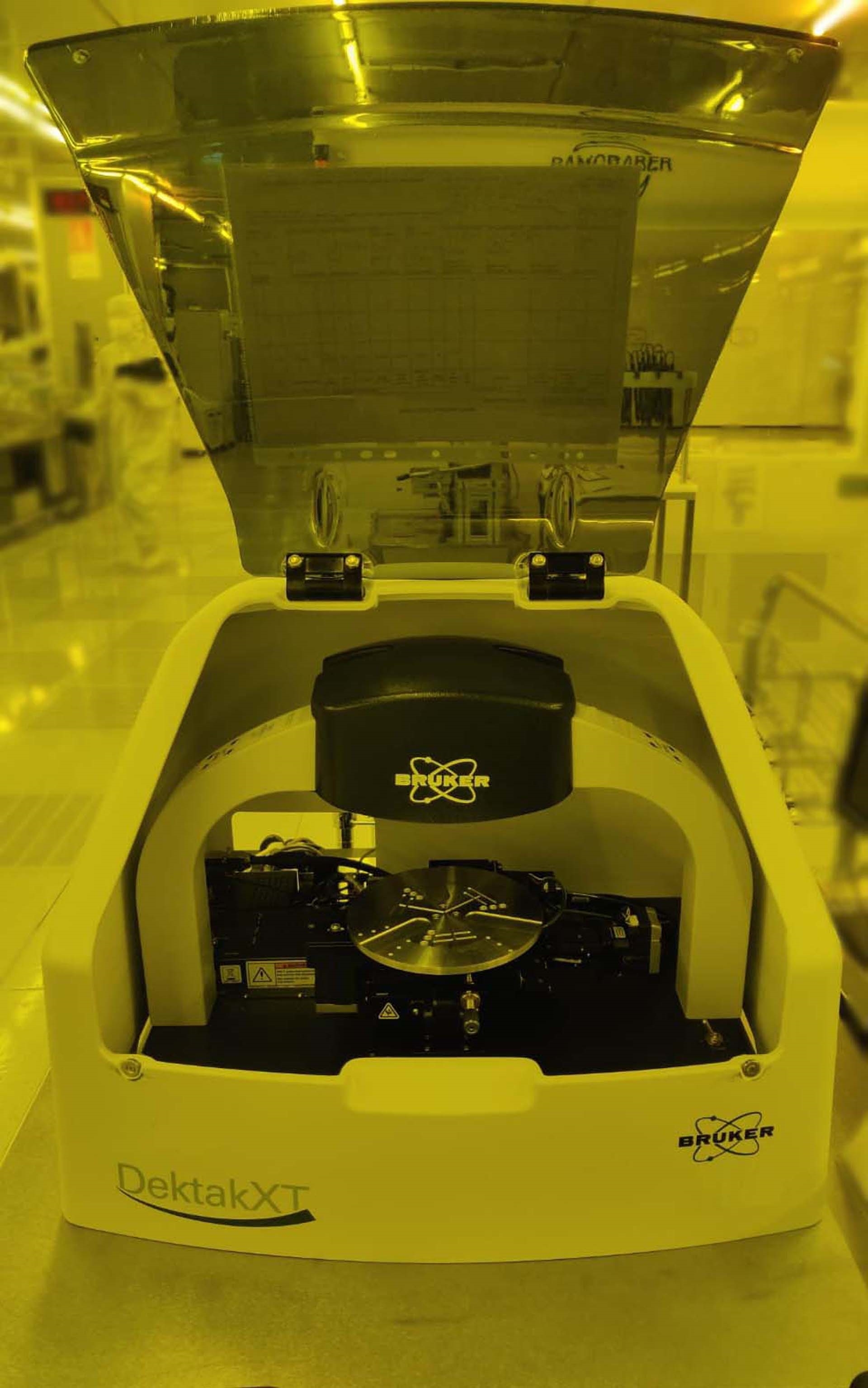
Used BRUKER-AXS Dektak XT #9238090 for sale
It looks like this item has already been sold. Check similar products below or contact us and our experienced team will find it for you.
Tap to zoom


Sold
ID: 9238090
Wafer Size: 8"
Vintage: 2012
Profiler, 8"
With PC
Stylus options:
Stylus radius: 50 nm - 25 pm
High Aspect Ratio (HAR): 200 pm x 20 pm
X/Y Manual leveling:
Manual: 100 mm
Motorized: 150 mm
Sample R-Θ stage:
Manual: Continuous 360°
Motorized: Continuous 360°
Computer system:
64-Bit multi-core parallel processor
Operating system: Windows 9 / 7.0
Measurement technique: Stylus profilometer (contact measurement)
Measurement capability: 2D Surface profile measurements
Sample viewing: Digital magnification, 0.275 to 2.2 mm vertical FOV
Stylus sensor: Low Inertia Sensor (LIS 3)
Stylus force: 1-15 mg With LIS 3 sensor
Vibration isolation
Scan length range with scan stitching capability: 55 mm, 200 mm
Data points per scan: 120,000
Sample thickness: 50 mm
Step height repeatability: 4 A, 1σ, 51 pm (30 scans using a 12.5 pm stylus)
Vertical range: 1 mm
Vertical resolution: 1 A (6.55 pm range)
Input power: 100-240 VAC, 50-60 Hz
Humidity range: ≤80%
Vibration table included
Temperature range:
Operating range: 20°C & 25°C (68°F-77°F)
2012 vintage.
BRUKER-AXS Dektak XT is an advanced wafer testing and metrology equipment specifically designed for use in semiconductor manufacturing and metrology. This system offers automated measurements of both critical dimensions (CD) and surface topography parameters on wafers up to 200mm for both silicon and compound semiconductor materials. The unit employs advanced techniques such as Step Height Analysis for high resolution topography measurements and Form Registration (FR) for very accurate step height and terrain measurements. Additionally, BRUKER-AXS DEKTAKXT can measure a number of electrical characteristics such as resistance, capacitance, and surface barrier resistances. Dektak XT utilizes high-precision metrology tools to provide sub-angstrom accuracy in determining nanoscale features on wafers. The efficient machine includes a computer controlled z-motion drive and a precision x-motion guide to accurately measure small features on wafers without sacrificing speed. DEKTAKXT is optimized for measuring microstructures and nanostructures, having a working range of 10μm to 50 μm. In addition to the precise measurements for wafers, BRUKER-AXS Dektak XT includes an ergonomic design featuring wide, unobstructed access to the area underneath the stage for the unequalled coverage required for today's thin wafers. An array of imaging capabilities are provided by the confocal optics which can measure features up to 40 μm. A scanning head allows configuration of spot sizes ranging from 10 μm to 200 μm. BRUKER-AXS DEKTAKXT is a highly precise automated metrology tool optimized for semiconductor fabrication. Advanced features such as Step Height Analysis and Form Registration allow for accurate measurement of nanoscale and microscale features on wafers. Its efficient motion control allows for sub-angstrom precision at maximum speed. The ergonomic design provides easy access to the area underneath the stage for managing quick and precise measurements efficiently. An assortment of imaging capabilities and spot sizes further adds to Dektak XT's versatility and facilitates efficient measurements for today's intricate semiconductor devices.
There are no reviews yet