Used CAMECA Lexfab 300 #293712655 for sale
URL successfully copied!
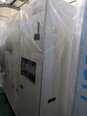
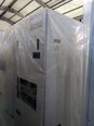
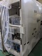
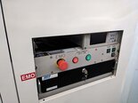








Tap to zoom
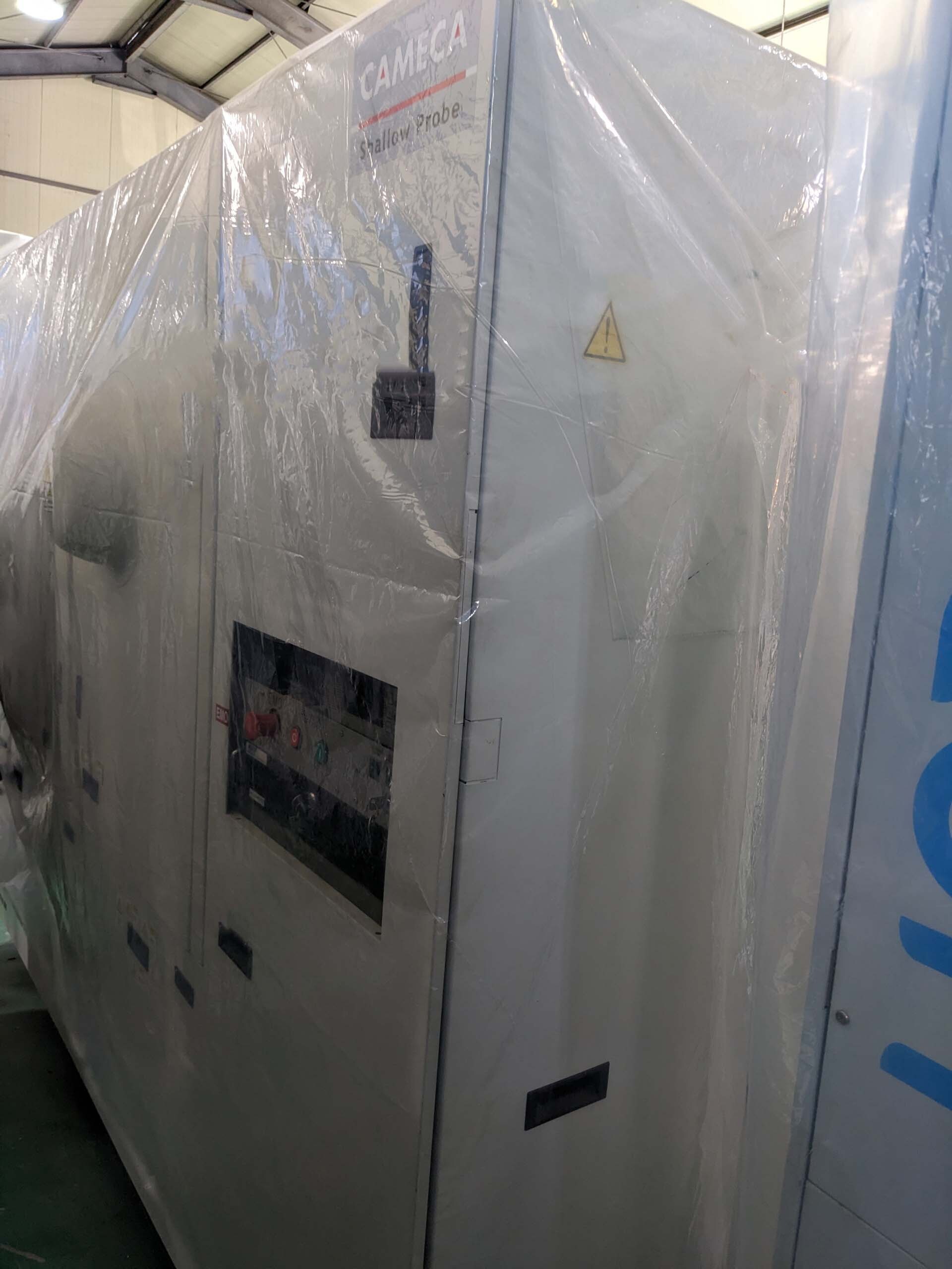

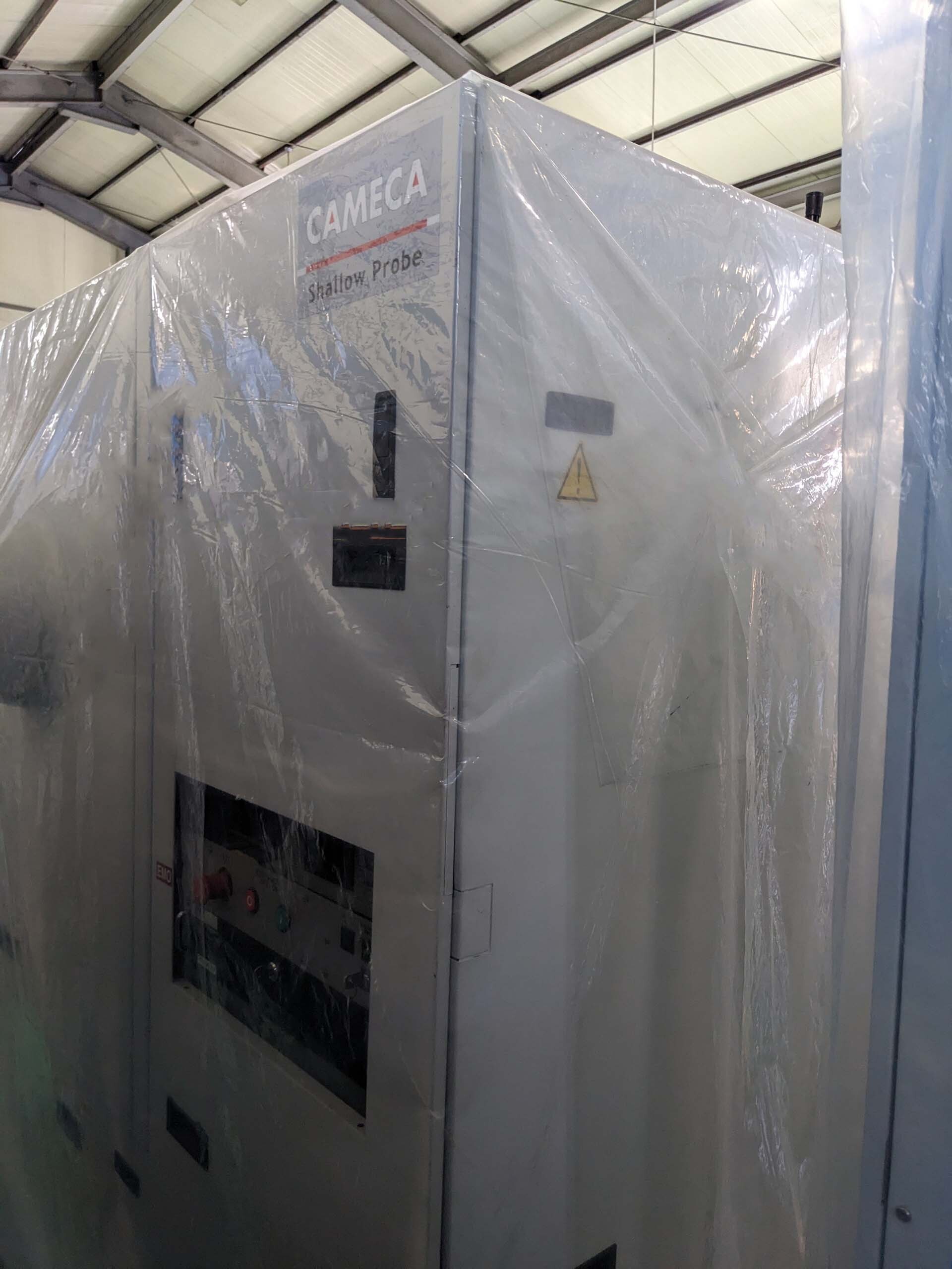
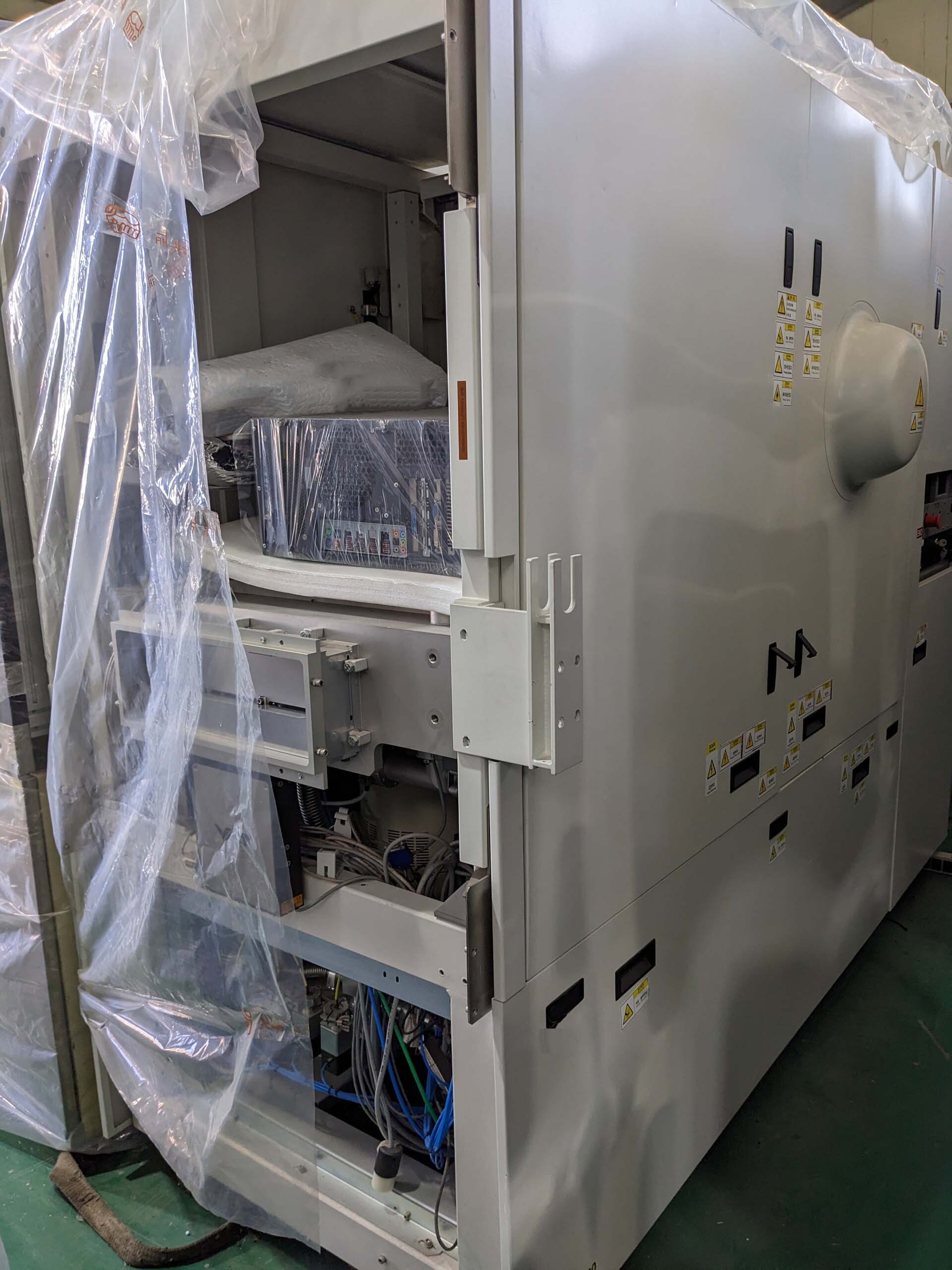
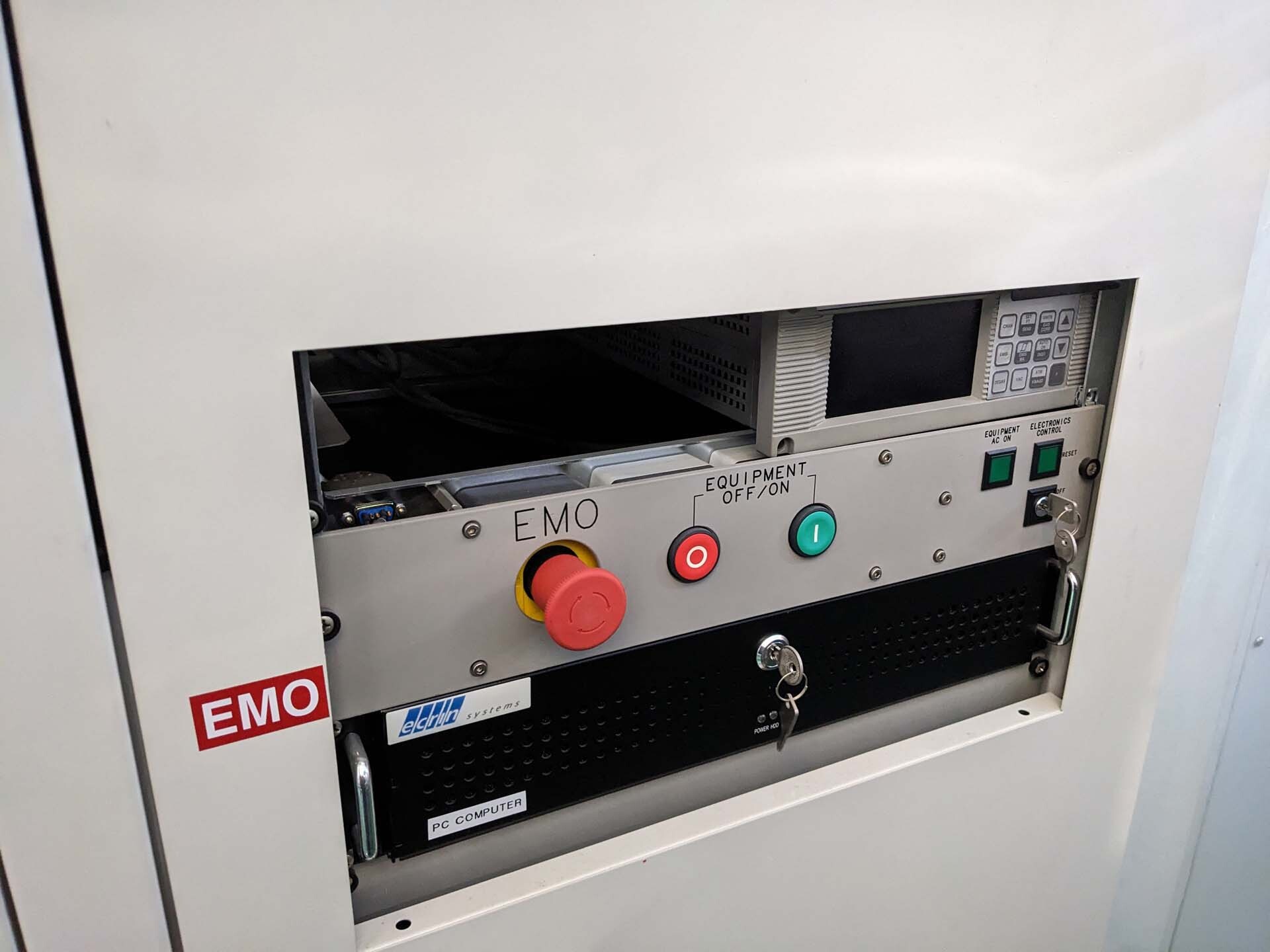
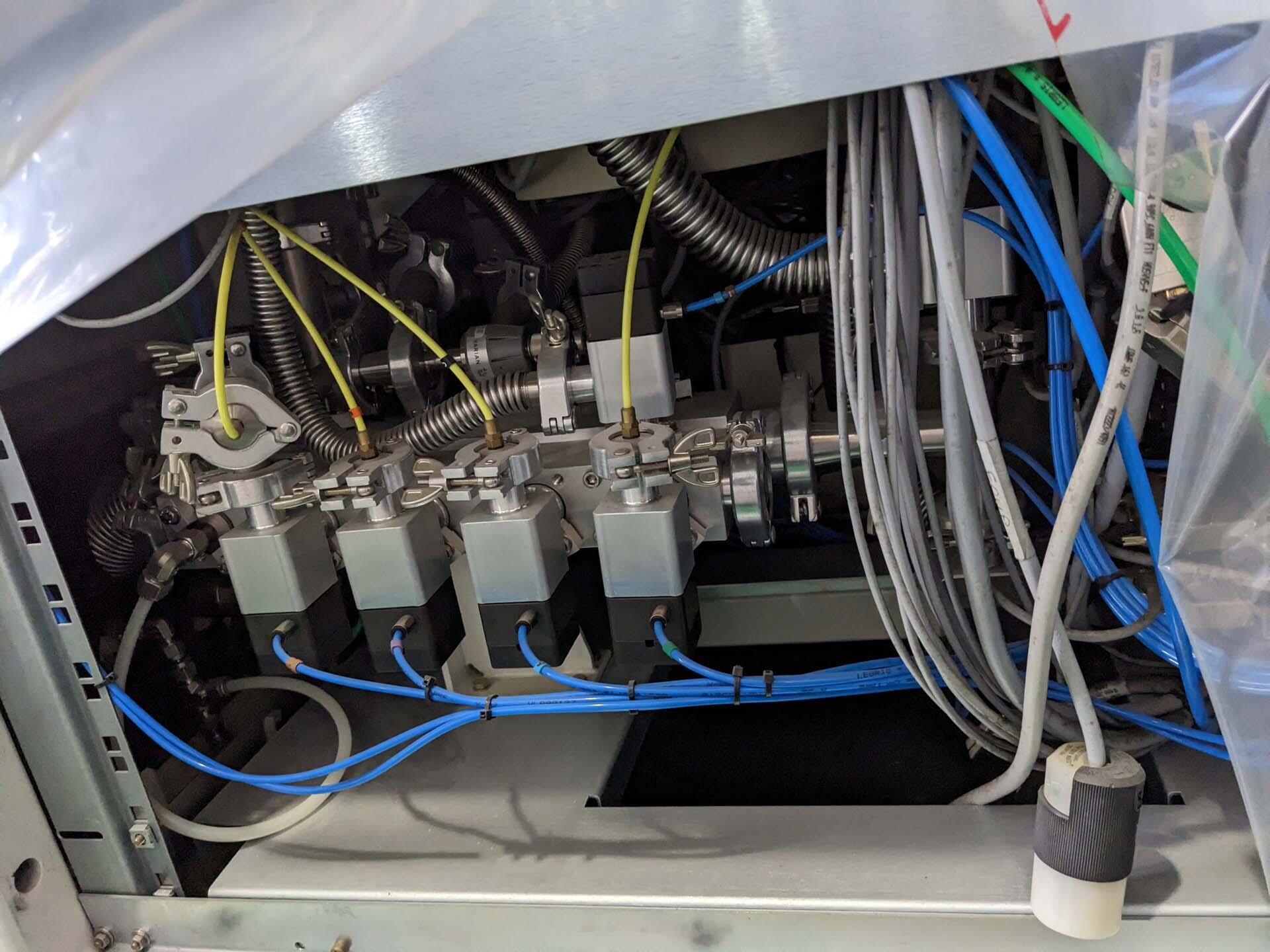
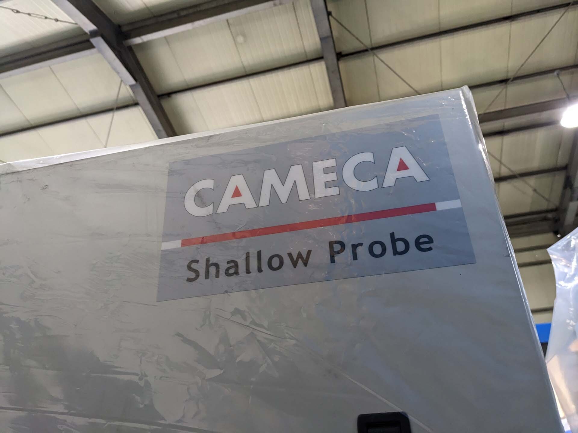

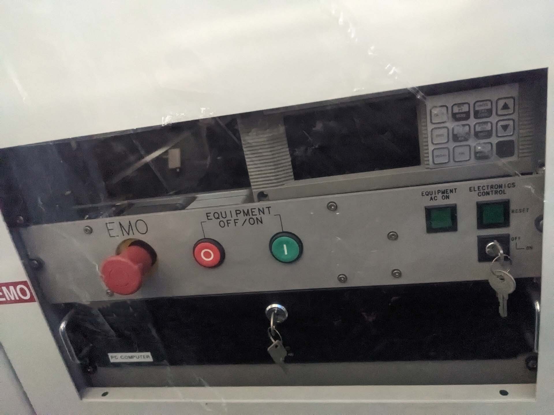
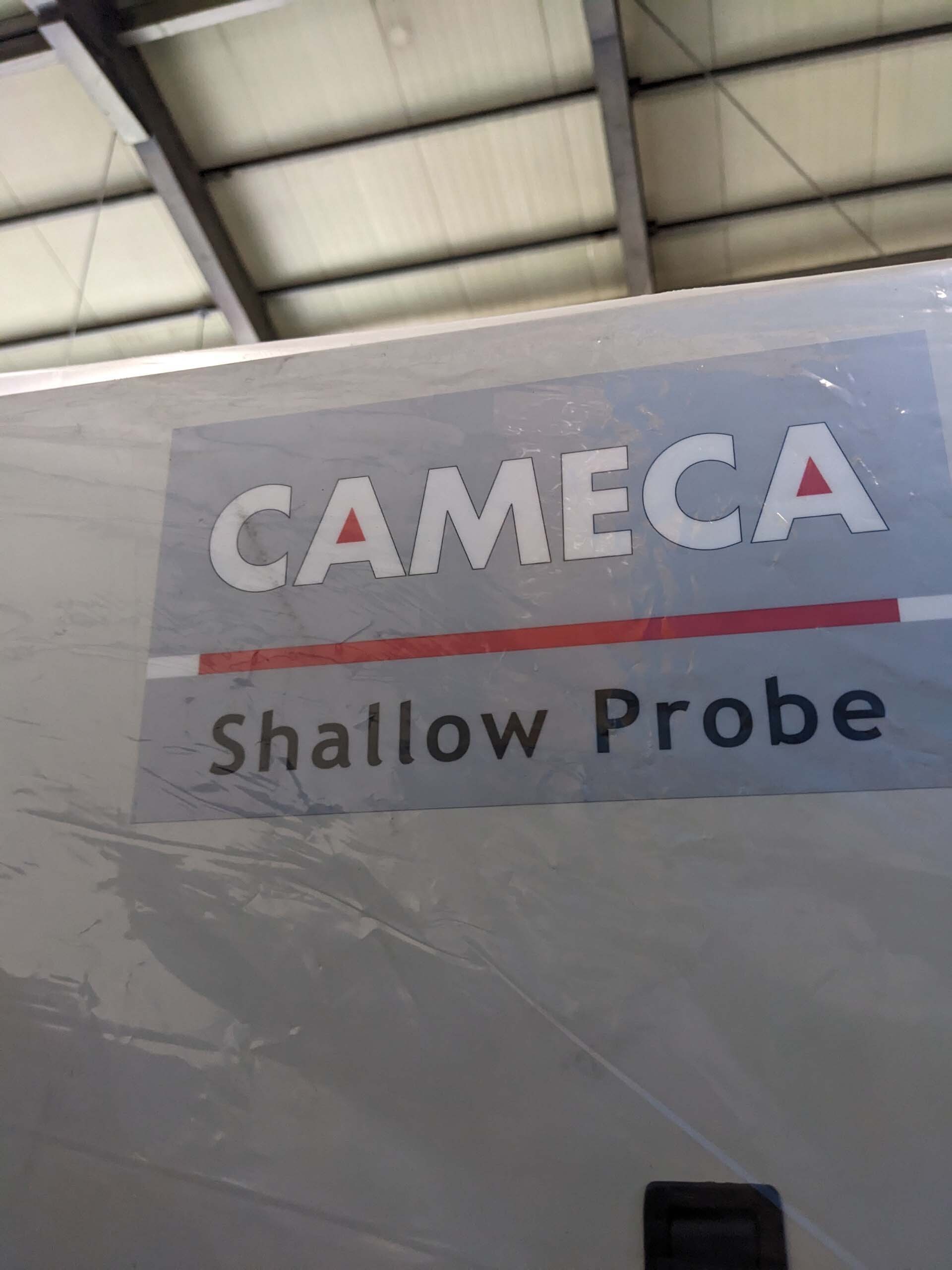
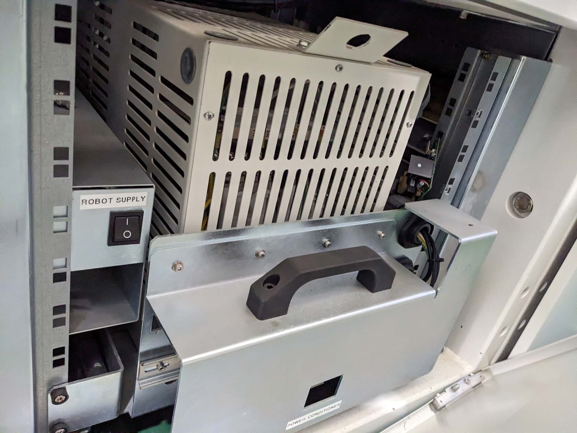
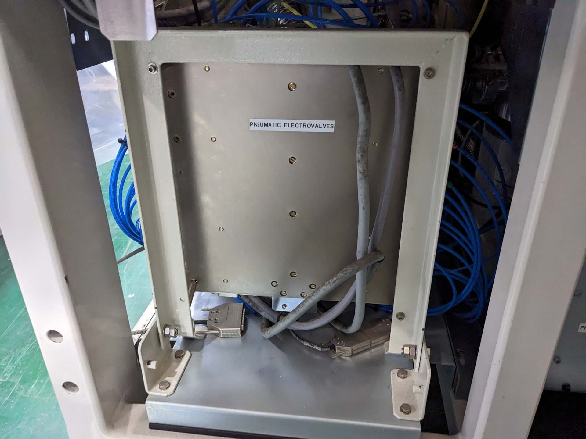
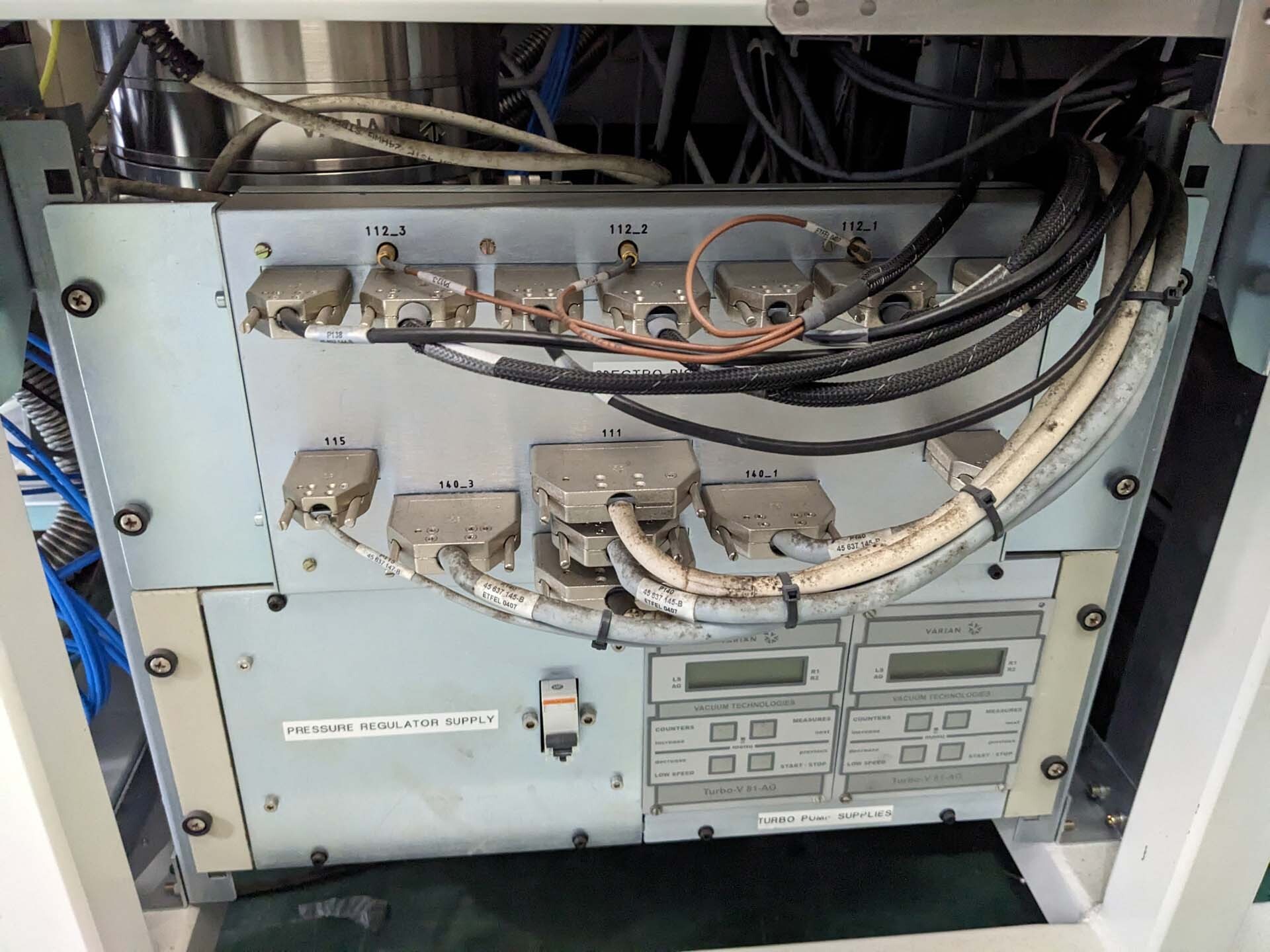
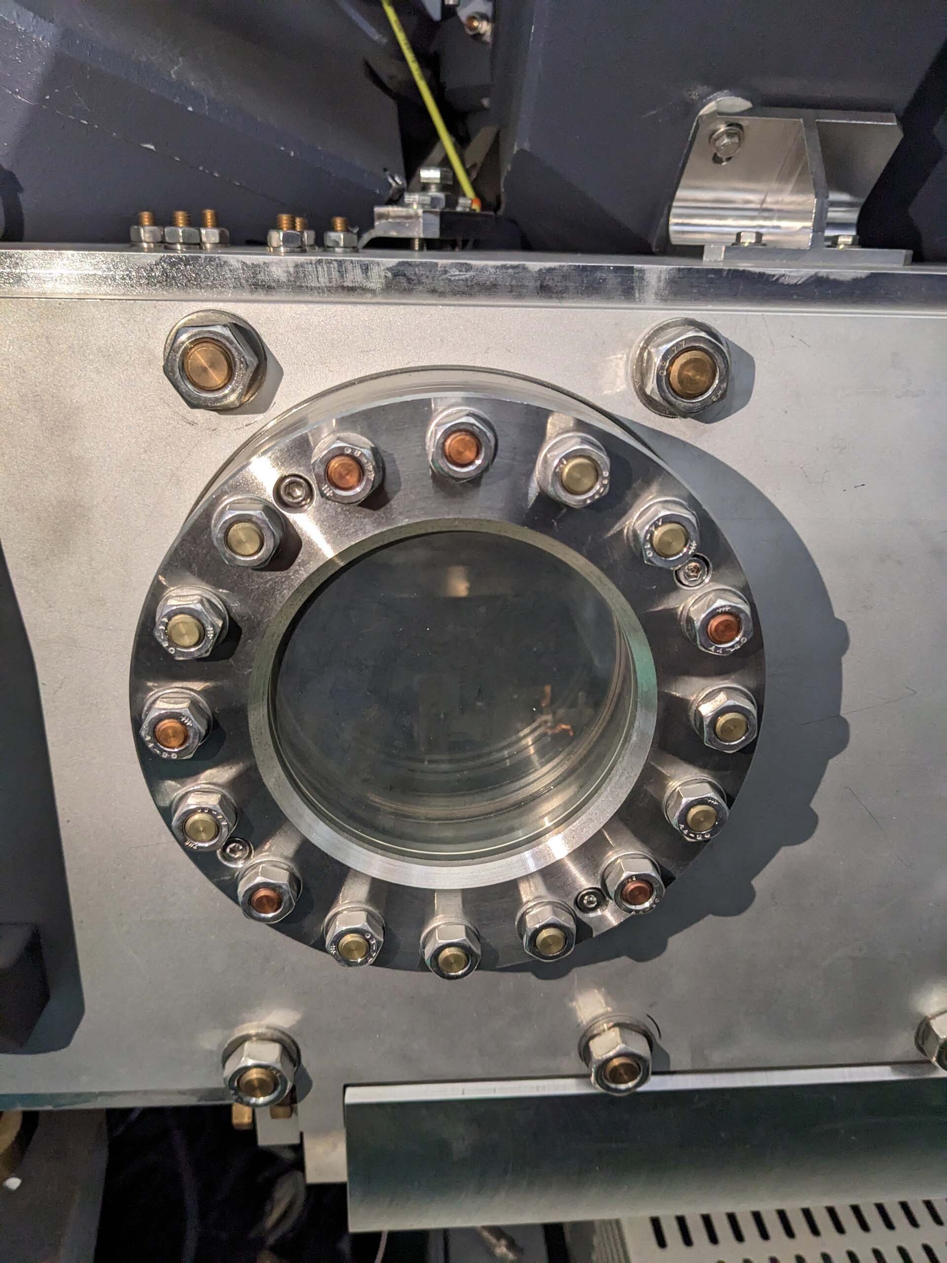
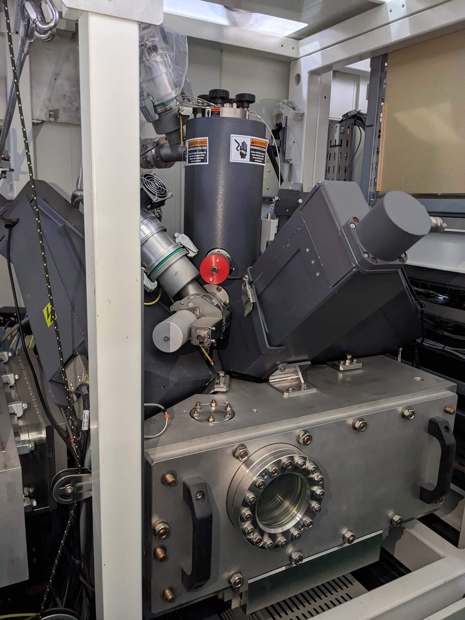
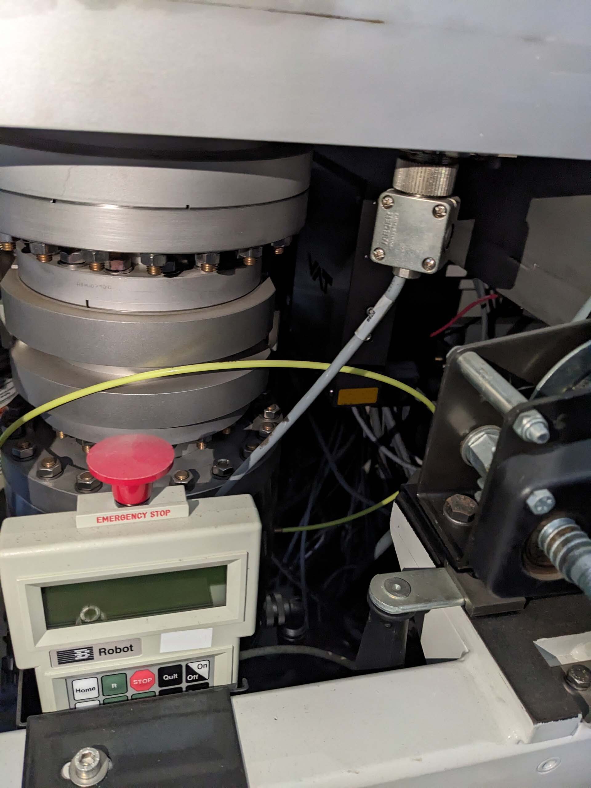
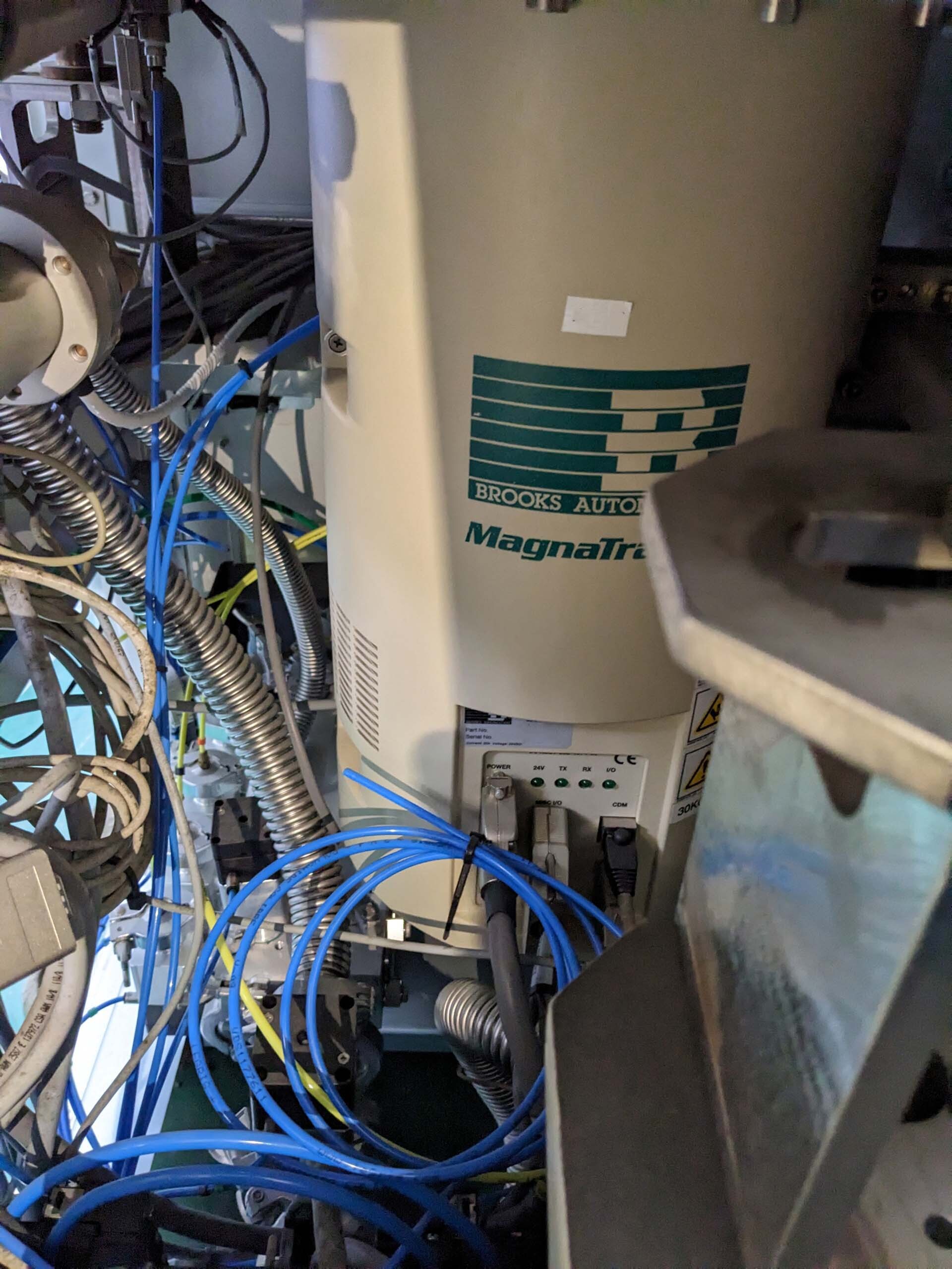
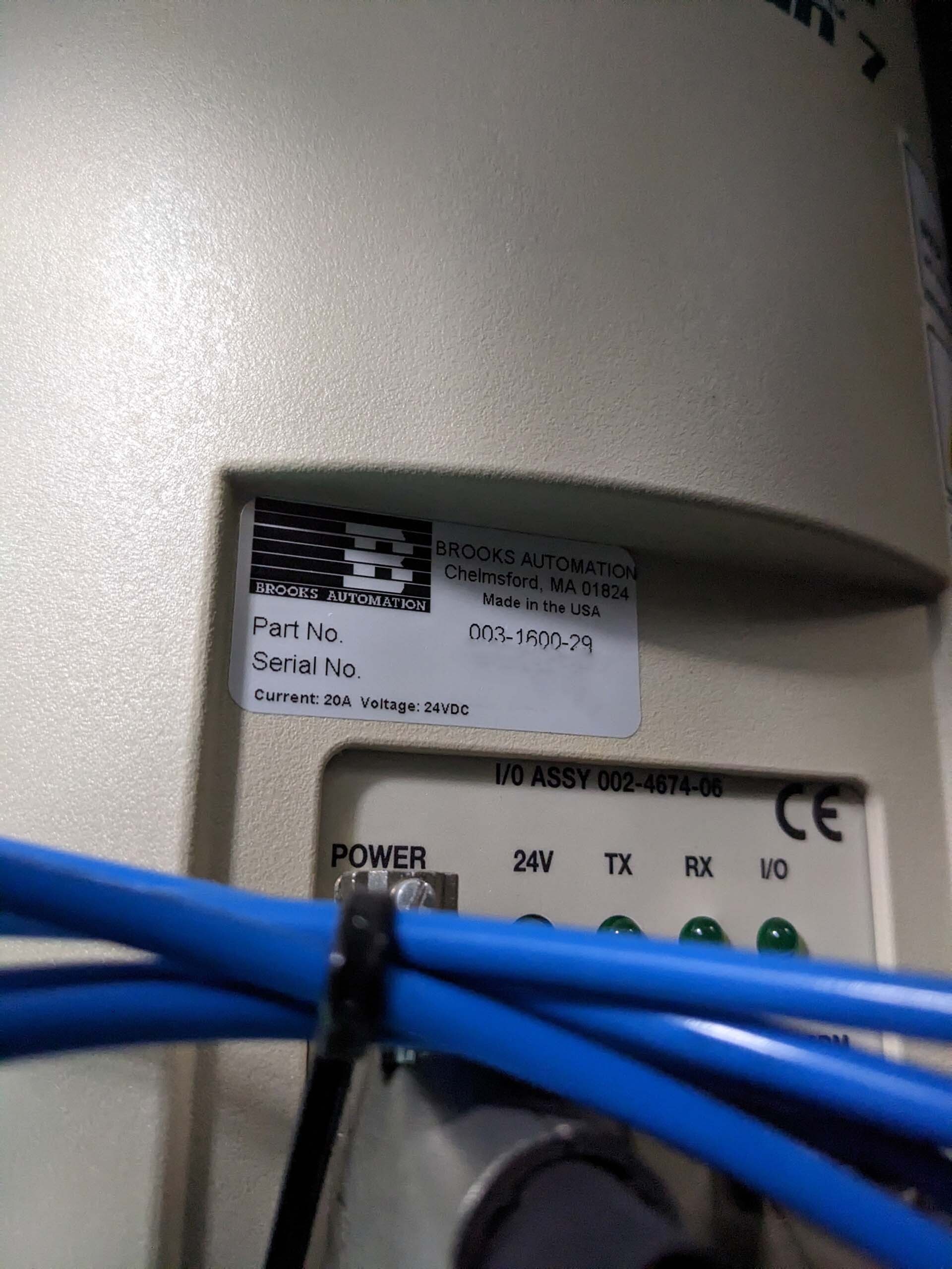
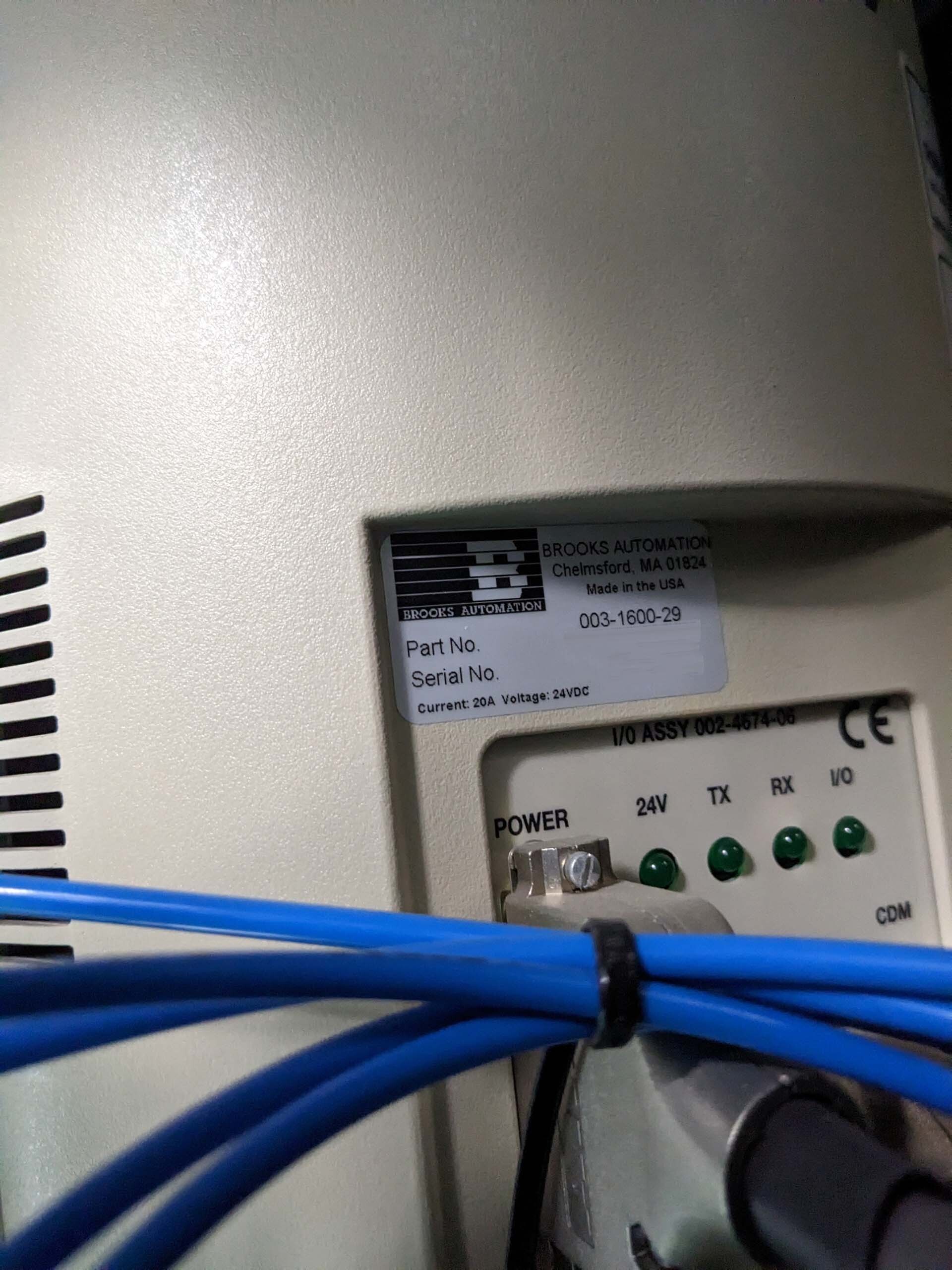
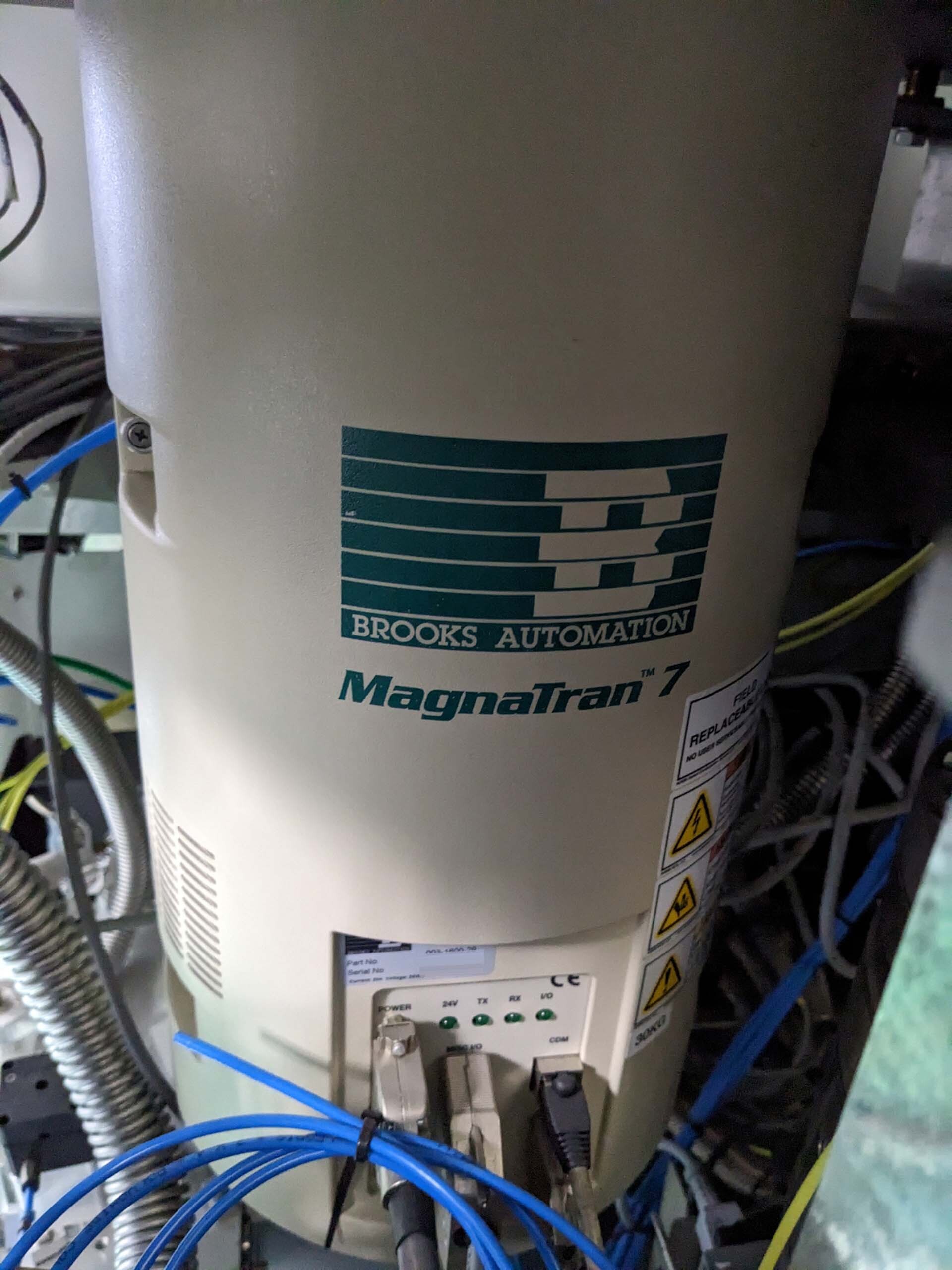
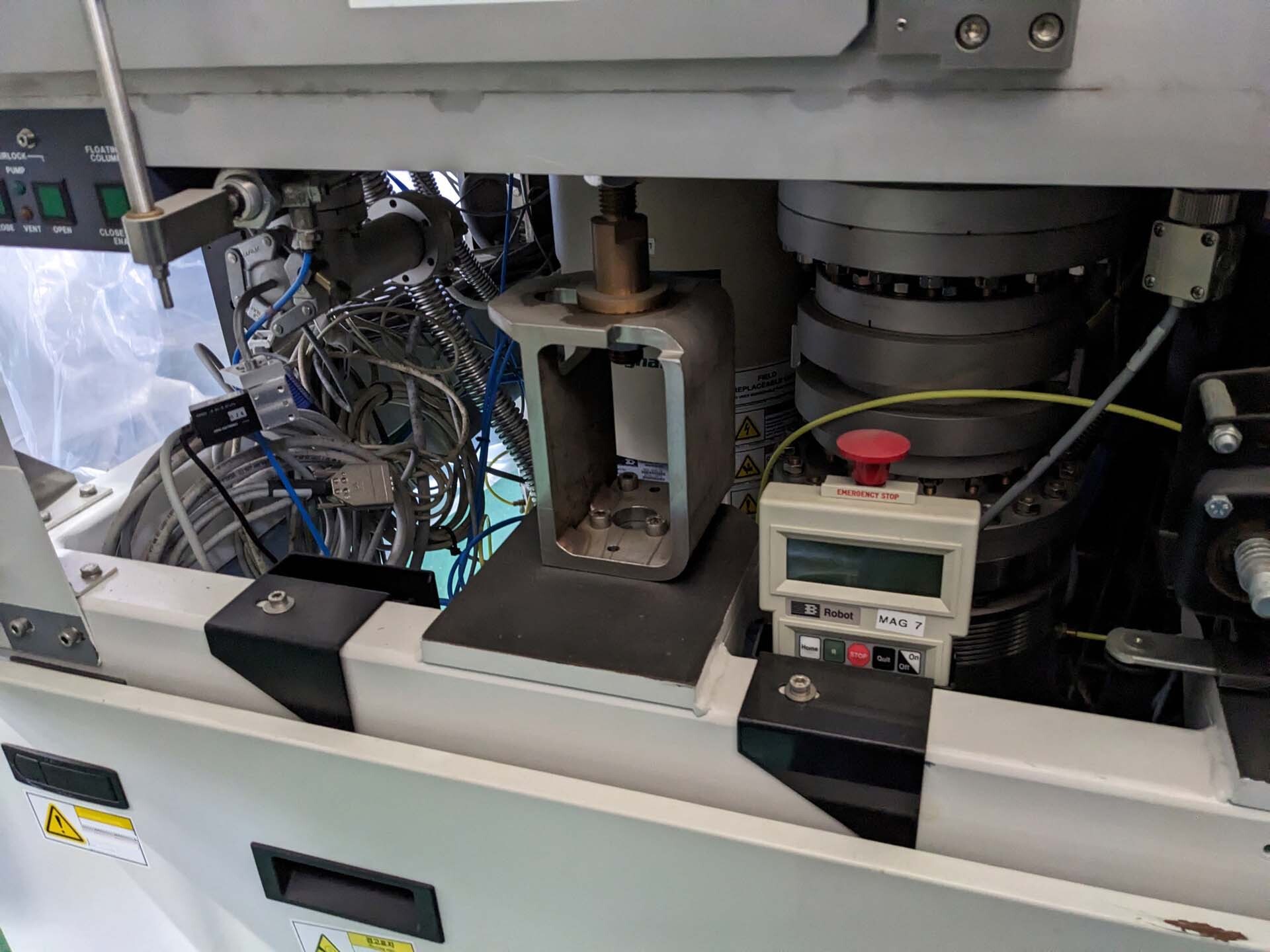
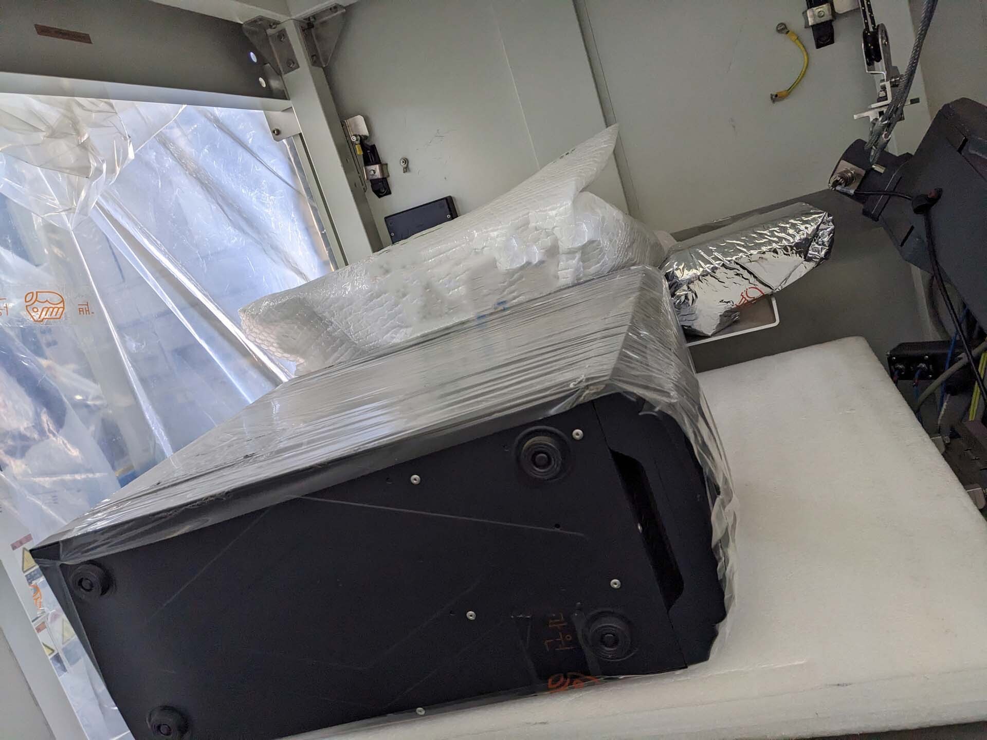
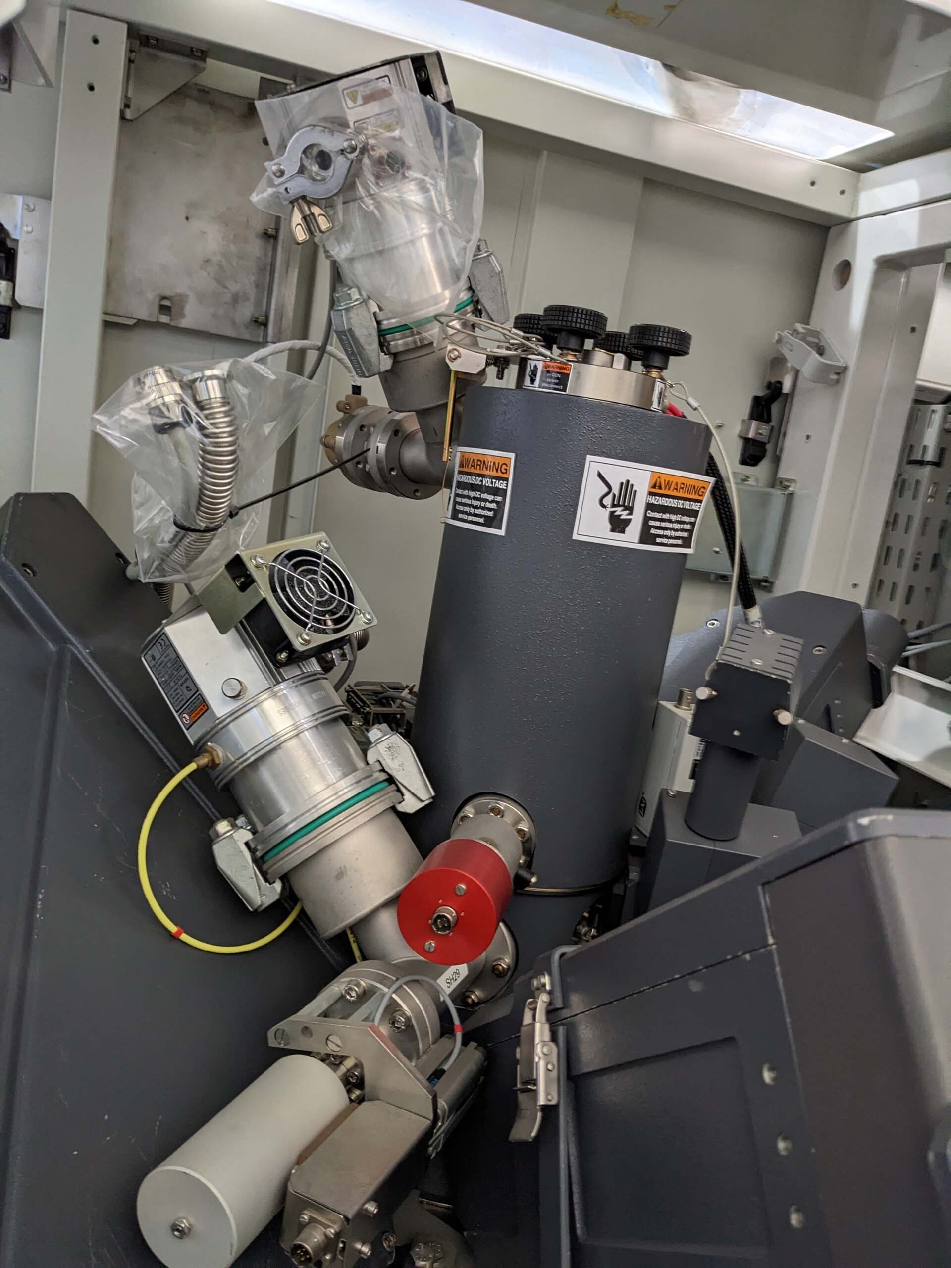
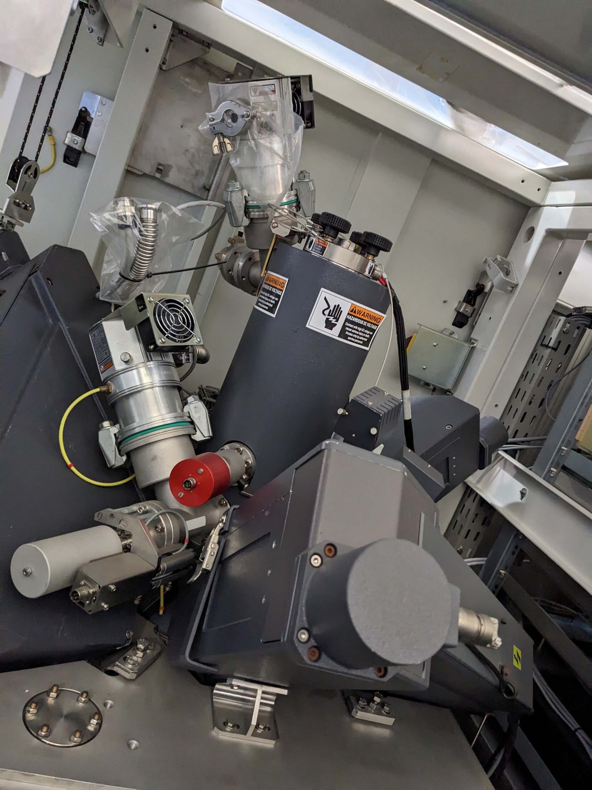
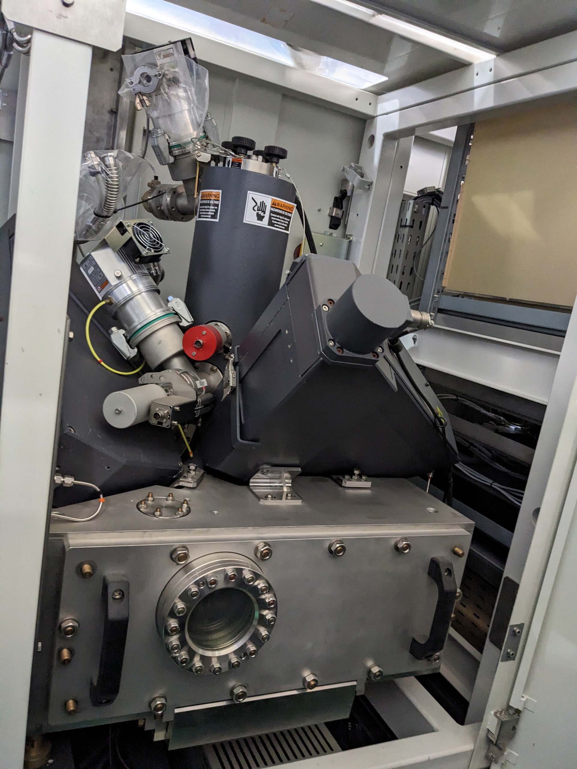
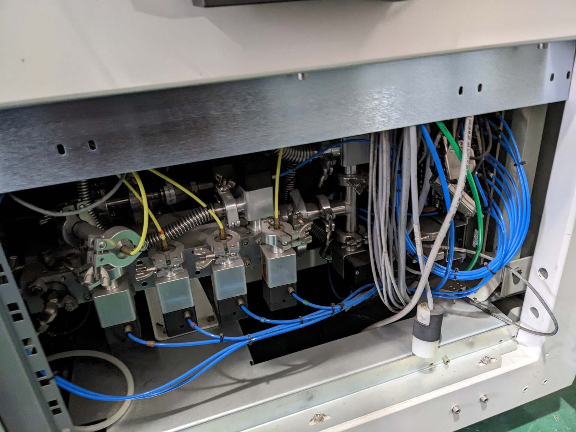
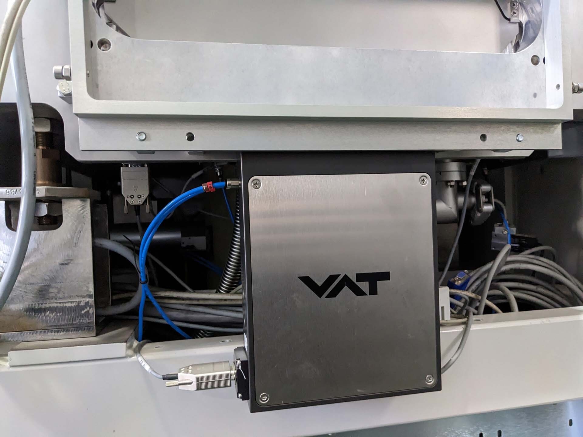
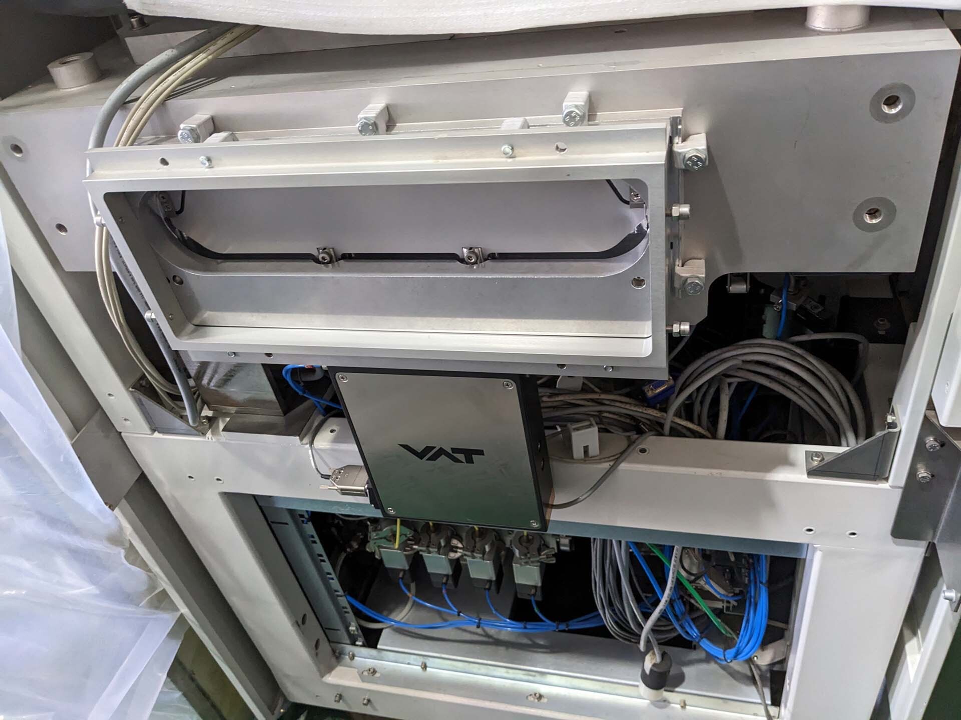
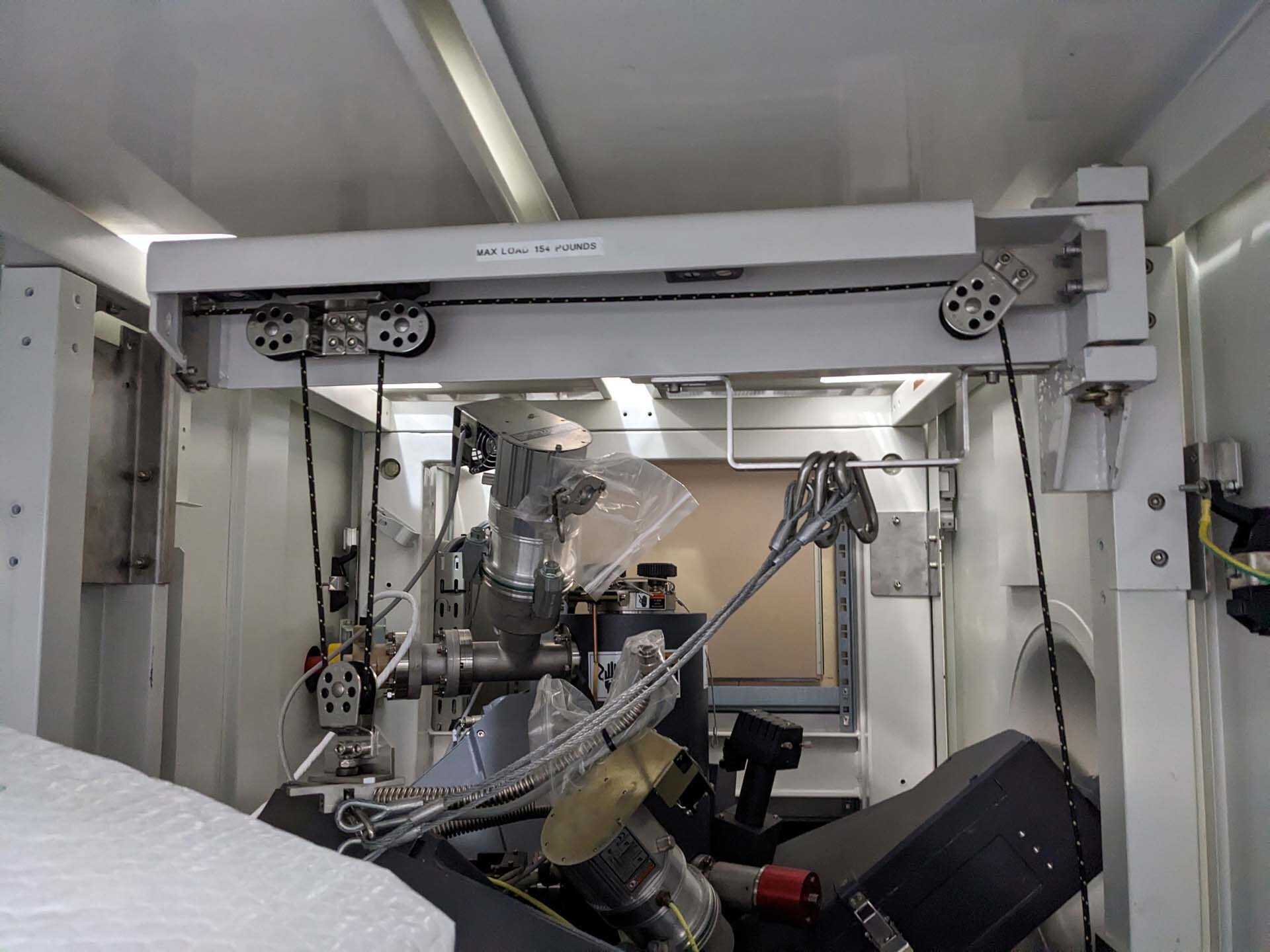
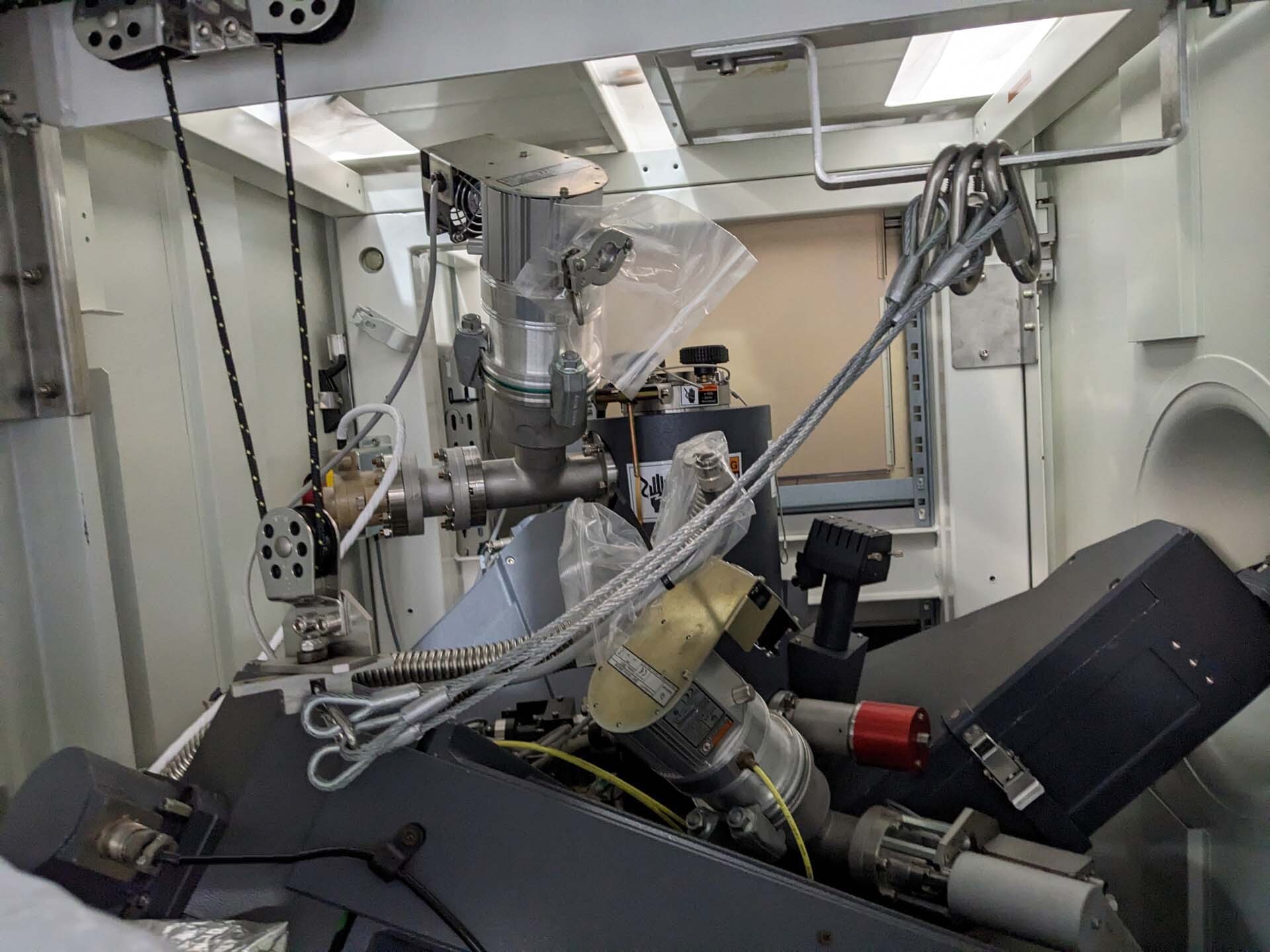
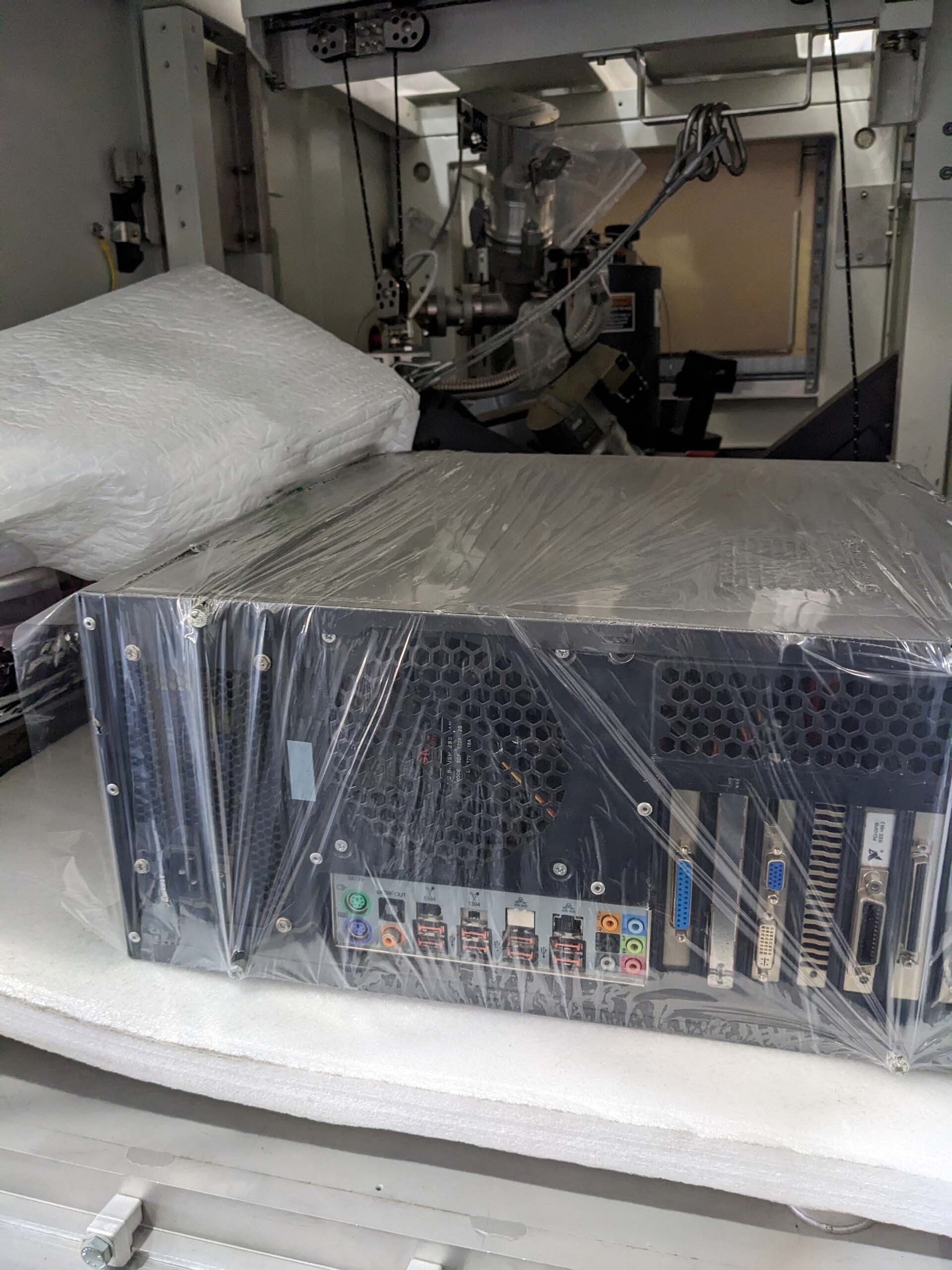
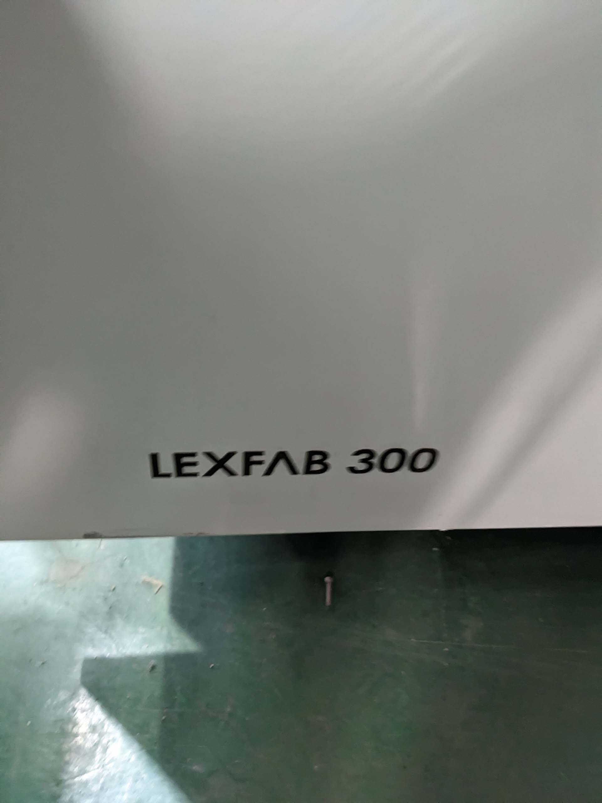
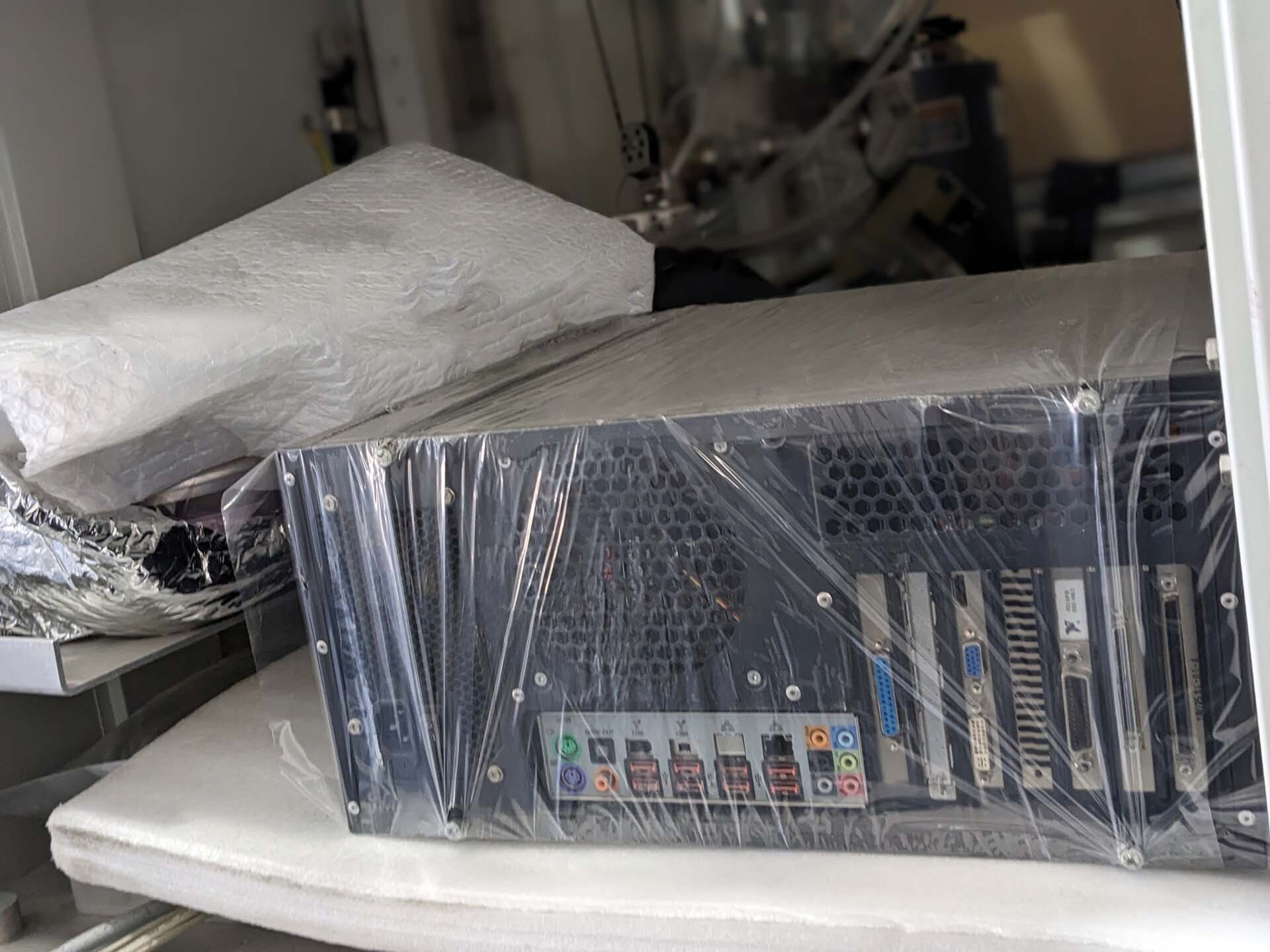
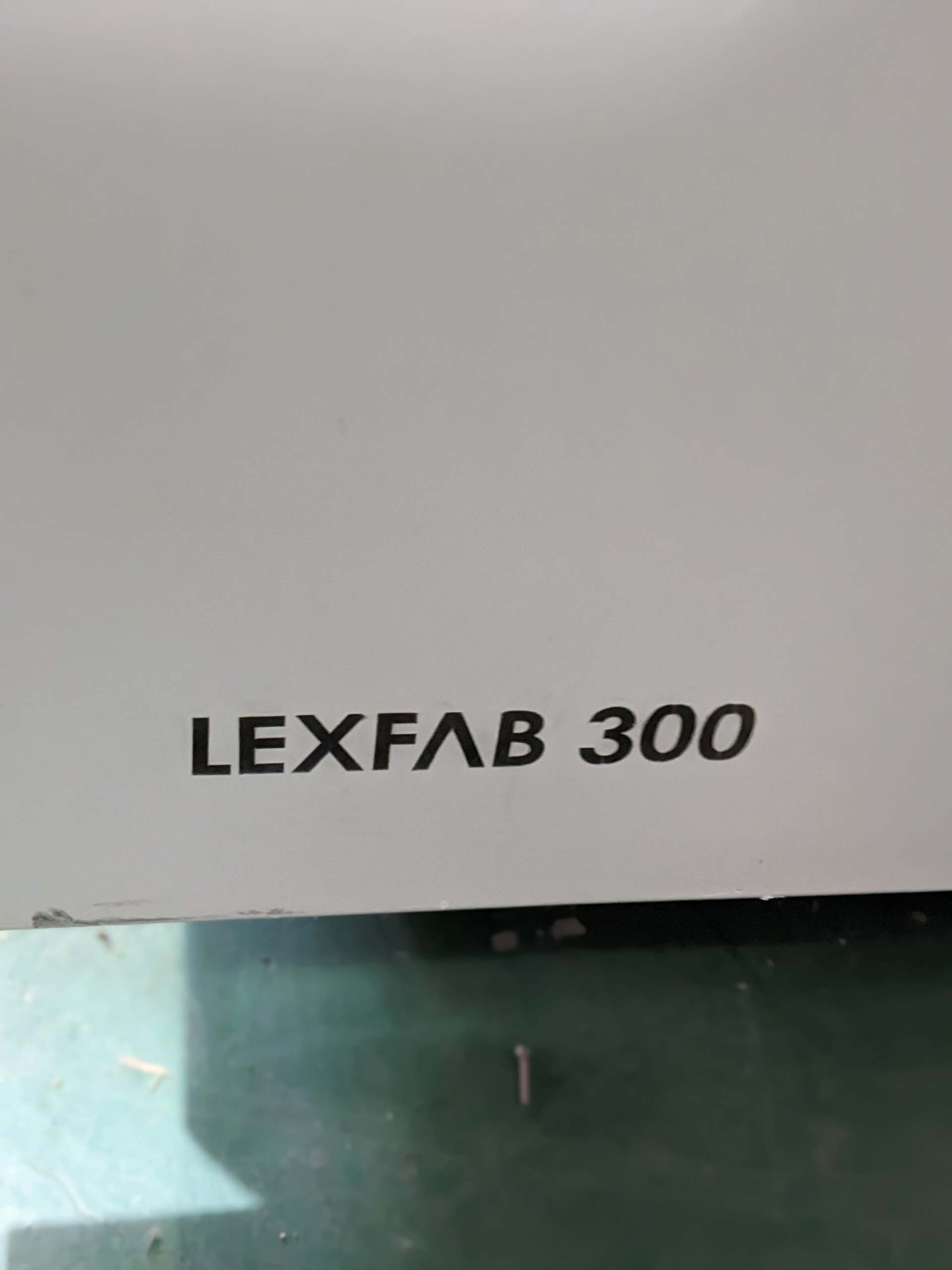
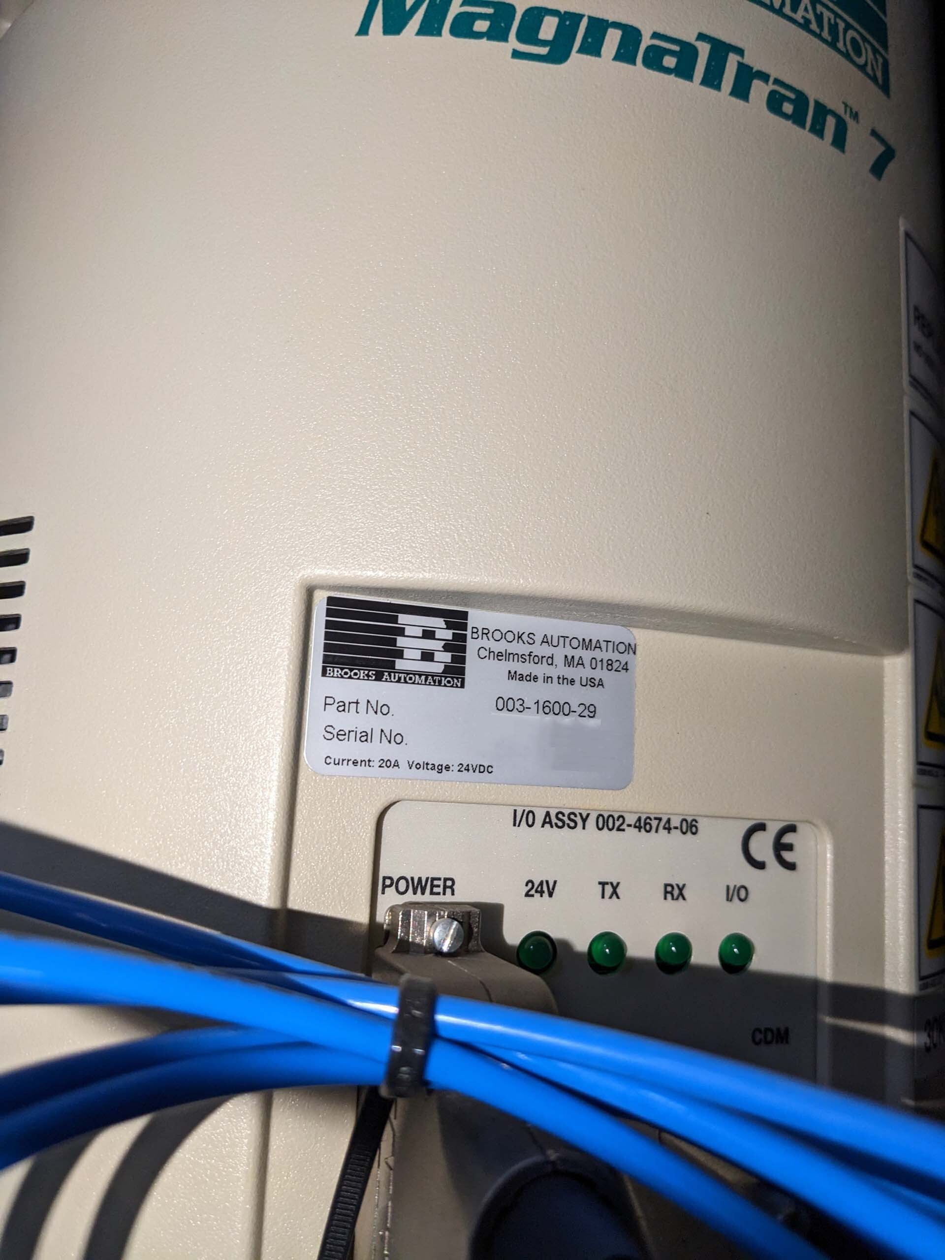
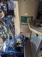
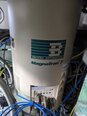
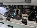
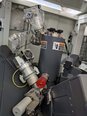
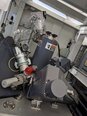
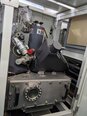
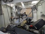
CAMECA Lexfab 300 is a state-of-the-art wafer testing and metrology equipment designed for advanced semiconductor manufacturing and research applications. This cutting-edge system integrates advanced technologies to provide precise and comprehensive measurement capabilities for characterizing semiconductor materials and devices. With its highly advanced functionalities and intuitive user interface, CAMECA LEXFAB300 offers a wide range of capabilities for analyzing semiconductor wafers with unmatched precision and efficiency. At the core of LEXFAB-300 unit is its powerful analytical engine, which leverages cutting-edge techniques such as scanning electron microscopy (SEM), energy-dispersive X-ray spectroscopy (EDS), and cathodoluminescence imaging (CL) to provide high-resolution imaging and chemical analysis of semiconductor samples. This enables users to accurately characterize the composition and structure of materials at the nanoscale level, allowing for detailed investigations of defects, impurities, and other critical parameters that can impact device performance. One of the key features of LEXFAB300 is its advanced automation capabilities, which streamline the testing and metrology processes for increased productivity and efficiency. The machine is equipped with robotic handling systems that enable seamless wafer loading and unloading, reducing manual intervention and minimizing the risk of sample contamination. Additionally, the tool features sophisticated software algorithms that automate data acquisition and analysis, allowing users to generate detailed reports and insights rapidly. In terms of performance, Lexfab 300 offers exceptional sensitivity and accuracy for a wide range of measurement parameters. The SEM imaging module provides high-resolution imaging capabilities with sub-nanometer resolution, allowing users to visualize the fine structures and features of semiconductor materials with unparalleled clarity. The EDS asset offers precise elemental analysis, enabling users to identify and quantify the chemical composition of materials with exceptional sensitivity and specificity. Moreover, the cathodoluminescence imaging module of CAMECA LEXFAB-300 model offers unique insights into the optical properties of semiconductor materials. By capturing and analyzing the light emitted from the sample under electron beam excitation, users can gain valuable information about the distribution of defects, impurities, and other optically active features within the material. This capability is particularly useful for studying the photonic properties of materials and optimizing the design of advanced semiconductor devices. In conclusion, CAMECA Lexfab 300 is a sophisticated and versatile wafer testing and metrology equipment that combines cutting-edge technologies with advanced automation capabilities to deliver exceptional performance and analytical capabilities for semiconductor applications. With its high-resolution imaging, precise chemical analysis, and unique cathodoluminescence imaging capabilities, this system provides researchers and manufacturers with a powerful tool for studying and optimizing semiconductor materials and devices with unprecedented detail and accuracy.
There are no reviews yet