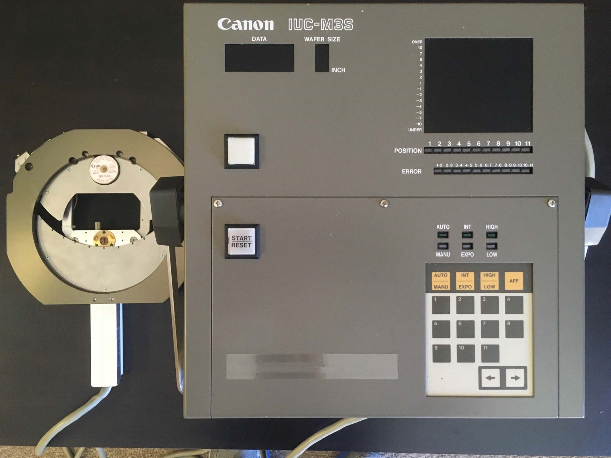
Used CANON IUC-M3S #9291909 for sale
URL successfully copied!
Tap to zoom


CANON IUC-M3S is a wafer testing and metrology equipment designed to provide users with accurate and precise wafer measurements and surface evaluations. The system is ideal for the semiconductor industry due to its ability to analyze wafers from both sides and the flexibility of the unit as an integrated solution. CANON IUC M 3 S wafer testing and metrology machine has a robust hardware tool, consisting of an ultrasound microscope, air-bearing sled, and data acquisition asset. The special ultrasound microscope, with its CCD camera, provides important information for the measurement and analysis of wafer surfaces. The air-bearing sled allows for precise and smooth movement of wafers under the microscope as well as transportation of wafers to and from the model. The data acquisition equipment is responsible for gathering and processing the measurements collected from the ultrasound microscope, such as the depth, width, height, and pitch of wafer surfaces. In addition, IUC-M3S has a comprehensive software system that provides users with detailed insights into wafer characteristics. Important functions such as wafer alignment, defect detection, surface classification, and error compensation are all made simple through the software. Moreover, the software is designed to maximize data throughput and support multiple data formats. IUC M 3 S wafer testing and metrology unit is designed with a focus on accuracy, precision, and reliability. The machine has a high-resolution camera that is capable of monitoring wafer surfaces to within 2.5nm. CANON IUC-M3S is also a flexible tool, with analysis data available in both ASCII and CSV formats for easy compatibility with many different software suites. Finally, the software of CANON IUC M 3 S is able to compensate for manufacturing errors with its advanced algorithms that minimize the impact of such errors. In summary, IUC-M3S is a comprehensive wafer testing and metrology asset that is designed with precision, accuracy, reliability, and flexibility in mind. The hardware model is composed of a robust ultrasound microscope, air-bearing sled, and data acquisition equipment, while the accompanying software system has numerous features that maximize data throughput and provide insights into wafer characteristics. The unit is capable of measuring and analyzing wafer surfaces within 2.5nm, and is designed to minimize the impact of manufacturing errors through its error compensation algorithms.
There are no reviews yet