Used CDE RESMAP 178 #293814715 for sale
URL successfully copied!
Tap to zoom
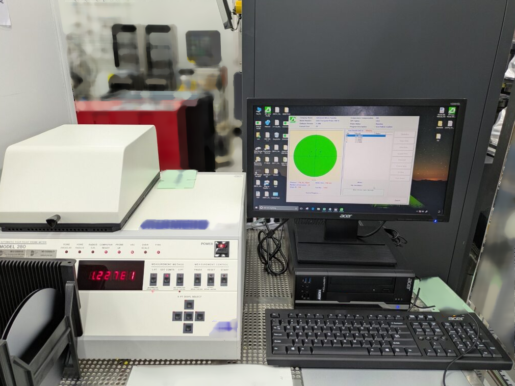

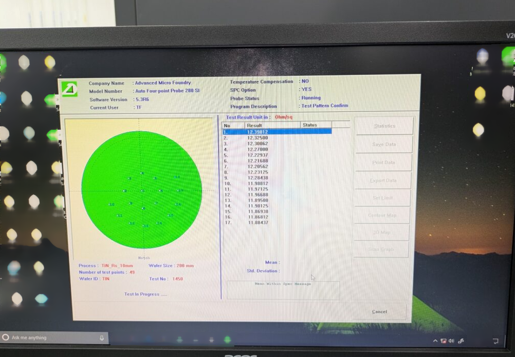
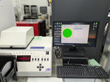
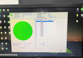
CDE RESMAP 178 is a next-generation wafer testing and metrology equipment specifically designed for reliable and high-accuracy critical dimension (CD) and overlay measurements. The system features an advanced opticaland two-dimensional non-contact surface imaging capability and with its multiple stages of calibration and alignment, it serves as a central measurement tool for modern semiconductor applications. The main component of the unit is a high-precision, computer-controlled wafer stage. This motion control machine provides precise motion control and positioning for both interaction and angle control. Unique, patented laser interferometric feature enables accurate mirror adjustment for angle and drift corrections. The U.V. laser source delivers high stability, power and accuracy. The mapping optical head consists of a high-resolution CCD camera, a rotating mirror, and a gradient-index (GRIN) lens, providing a magnified height/distance profile of the topography of a sample across the x-y plane. CDE RESMAP178 wafer testing and metrology tool offers two measurement devices, an X-stylus probe and an auto-styluswhich can measure a variety of samples. The X-stylus probe is especially suitable for the precise measurement of critical dimension and overlay alignment. The auto-stylus is designed for measuring both metal and dielectric layers which allow for precise measuring of thin metal lines without contact defect. Additionally, there is a High-Precision Wafer and Sample Mapping software that works in conjunction with a set of color-coded wafer mapping tables to display scan results. In terms of data processing, RESMAP 178 asset offers the possibility of real-time image grabbing, stitching, and edge detection. As for data format conversion, the user can directly transfer scan data into 3D representations and report formats, such as .csv, .txt and .xlsx. Statistics modules are available for graphics data analysis and display. Overall, RESMAP178 wafer testing and metrology model is a reliable and robust equipment that has been proven in a number of semiconductor industry applications. The system is highly flexible and user-friendly, offering real-time results and data analysis support. Utilizing the features of the unit, customers can ensure maximum throughput of the testing procedure and ensure that the output meets their desired precision and accuracy requirements.
There are no reviews yet