Used CDE RESMAP 178 #293821805 for sale
URL successfully copied!
Tap to zoom
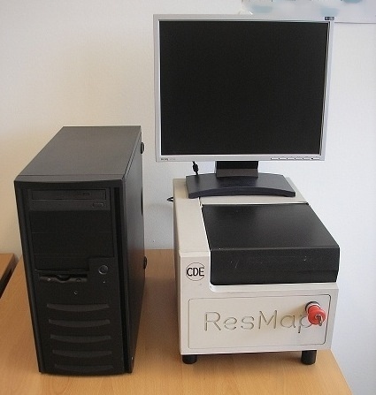

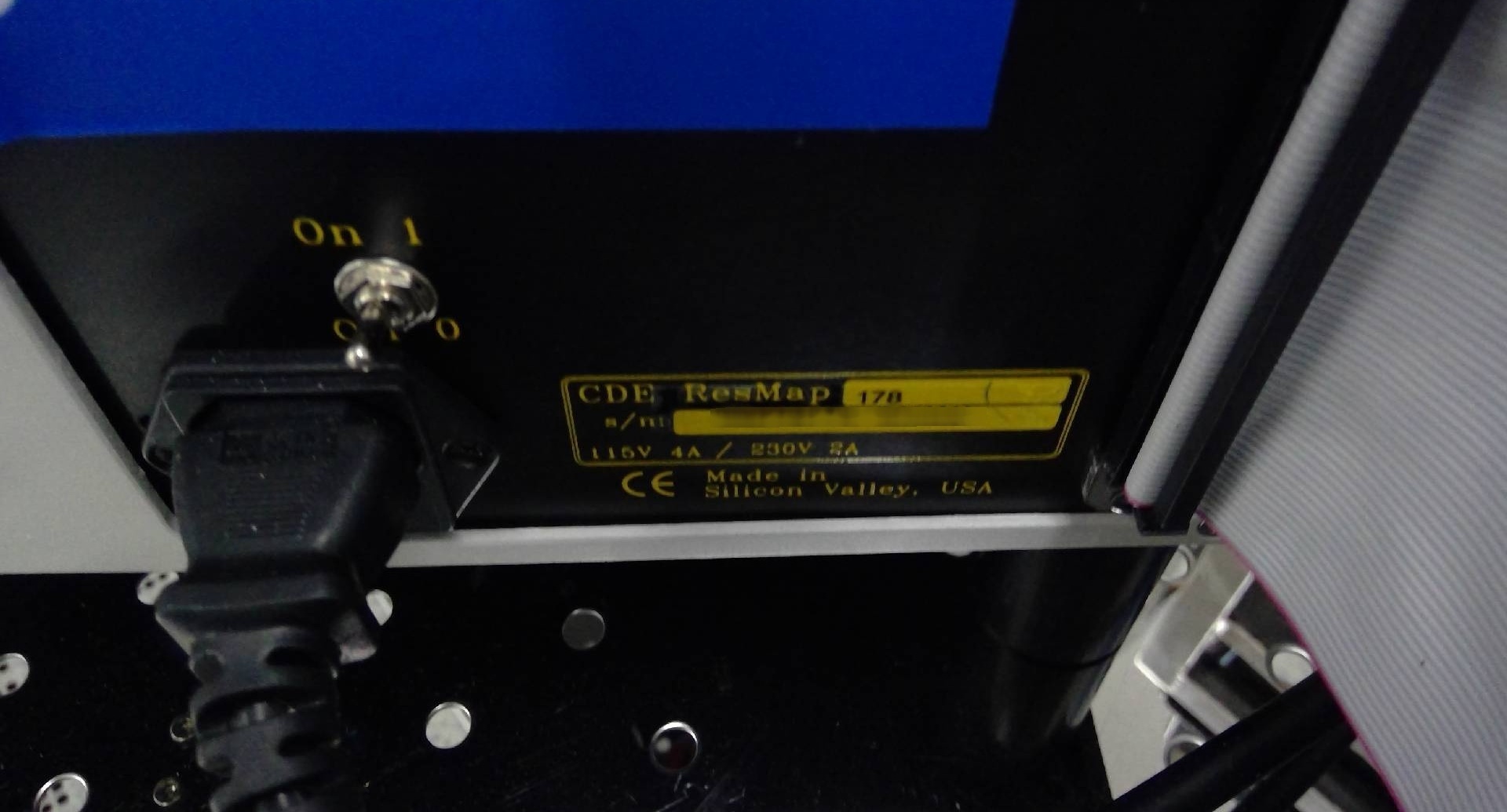
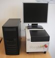
CDE RESMAP 178 is a state-of-the-art wafer testing and metrology equipment designed and manufactured by CDE, an international supplier of metrology systems. As its name suggests, CDE RESMAP178 is a multi-purpose system that offers a wide array of metrology and defect characterization capabilities. RESMAP 178 offers a variety of high-performance charge-coupled device (CCD) imaging technologies, including both bright-field and dark-field captured images. These images can be used to detect and measure the size and shape of wafer defects, as well as other surface features. In addition, RESMAP178 offers advanced image processing algorithms that can be customized to meet a user's specific needs. The unit's electrical test capabilities also allow for the performance of static and/or dynamic electrical tests on a wafer. By employing a combination of these tests, users can identify wafer defects and determine the characteristics of the electrical signals being transmitted. Furthermore, CDE RESMAP 178's high-precision, multi-channel potentiometer enables precise measurements of the voltage and current applied to a device for a given range of electrical parameters. Another major strength of CDE RESMAP178 is its robust wafer-handling capabilities. The machine accommodates a wide range of wafer sizes, types, and thicknesses. It also features a unique automated wafer-loading mechanism that enables faster and easier wafer loading and unloading. This feature eliminates the need for personnel to manually fine-tune the wafer-handling parameters. Finally, RESMAP 178 offers complete connectivity with a comprehensive database management tool (DBMS) and a graphical user interface (GUI). This allows users to store and manage test results, which can be used to develop new methods and enhance product quality. In addition, the DBMS and GUI are highly customizable, enabling users to tailor the asset to their specific needs. Overall, RESMAP178 is an advanced wafer testing and metrology model that is capable of performing accurate and reliable wafer measurements and defect characterization. Its wide range of features and capabilities make it an invaluable tool for ensuring quality and reliability in the semiconductor industry.
There are no reviews yet