Used CDE RESMAP 178 #293832078 for sale
URL successfully copied!
Tap to zoom
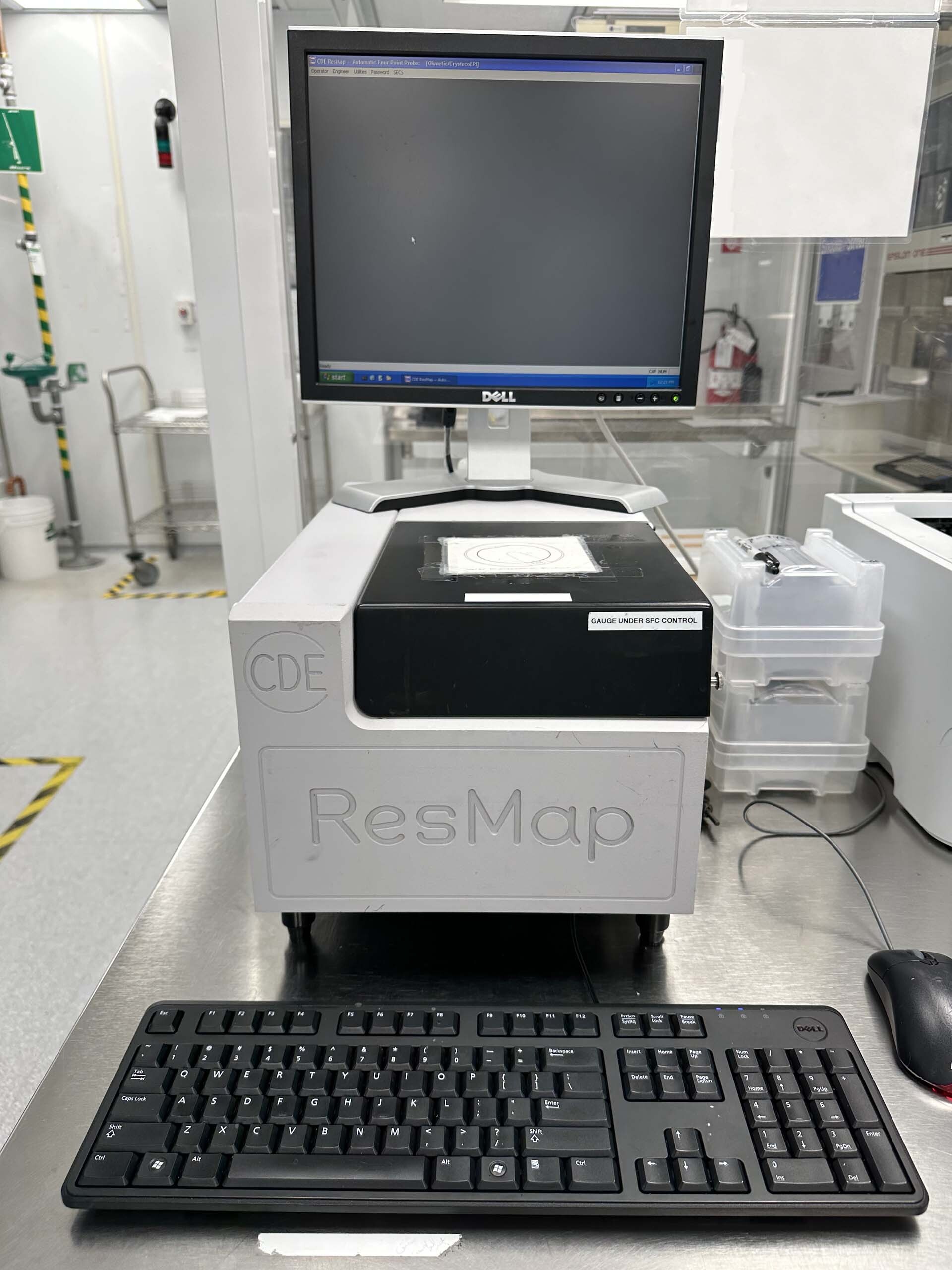

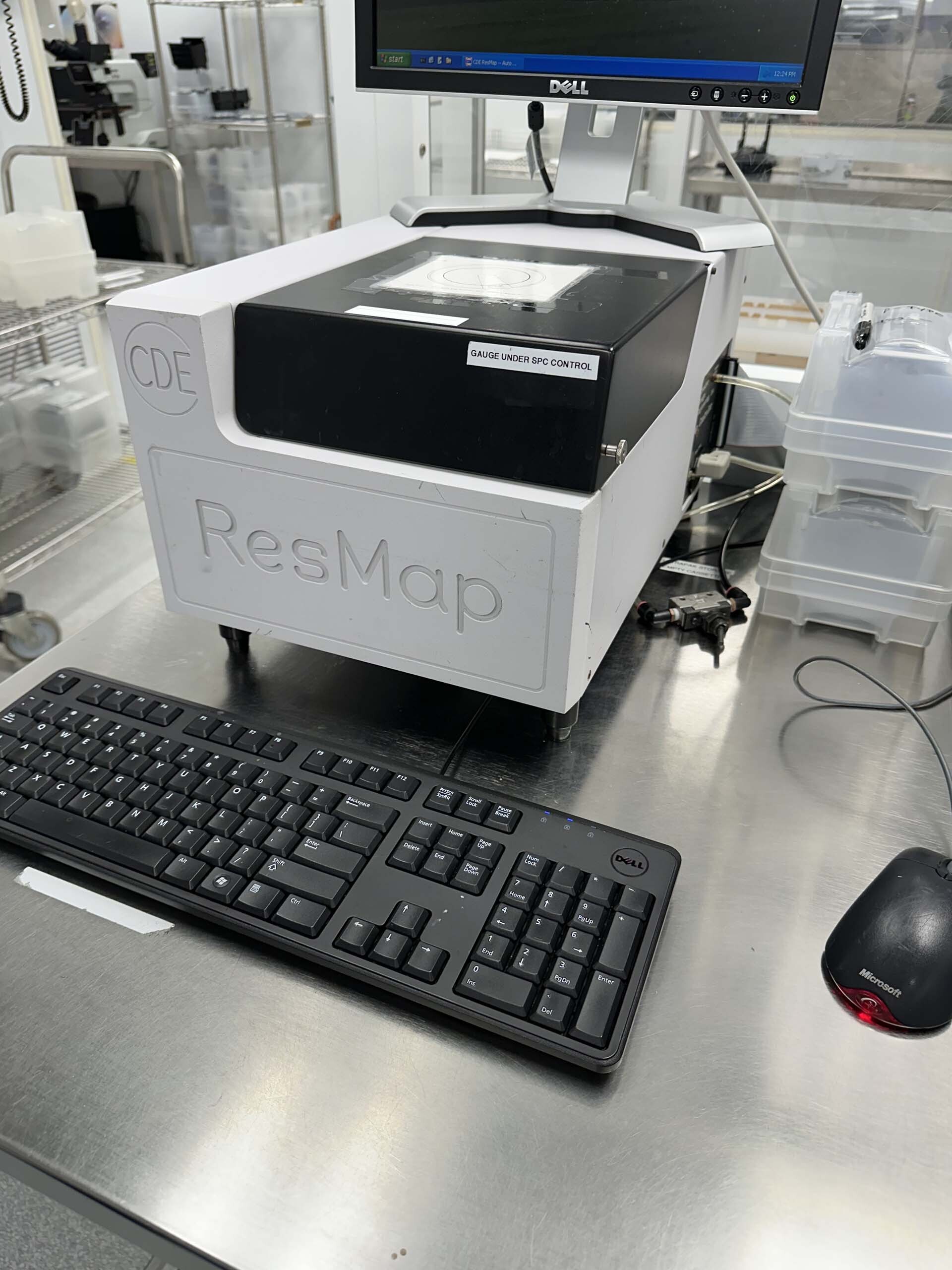
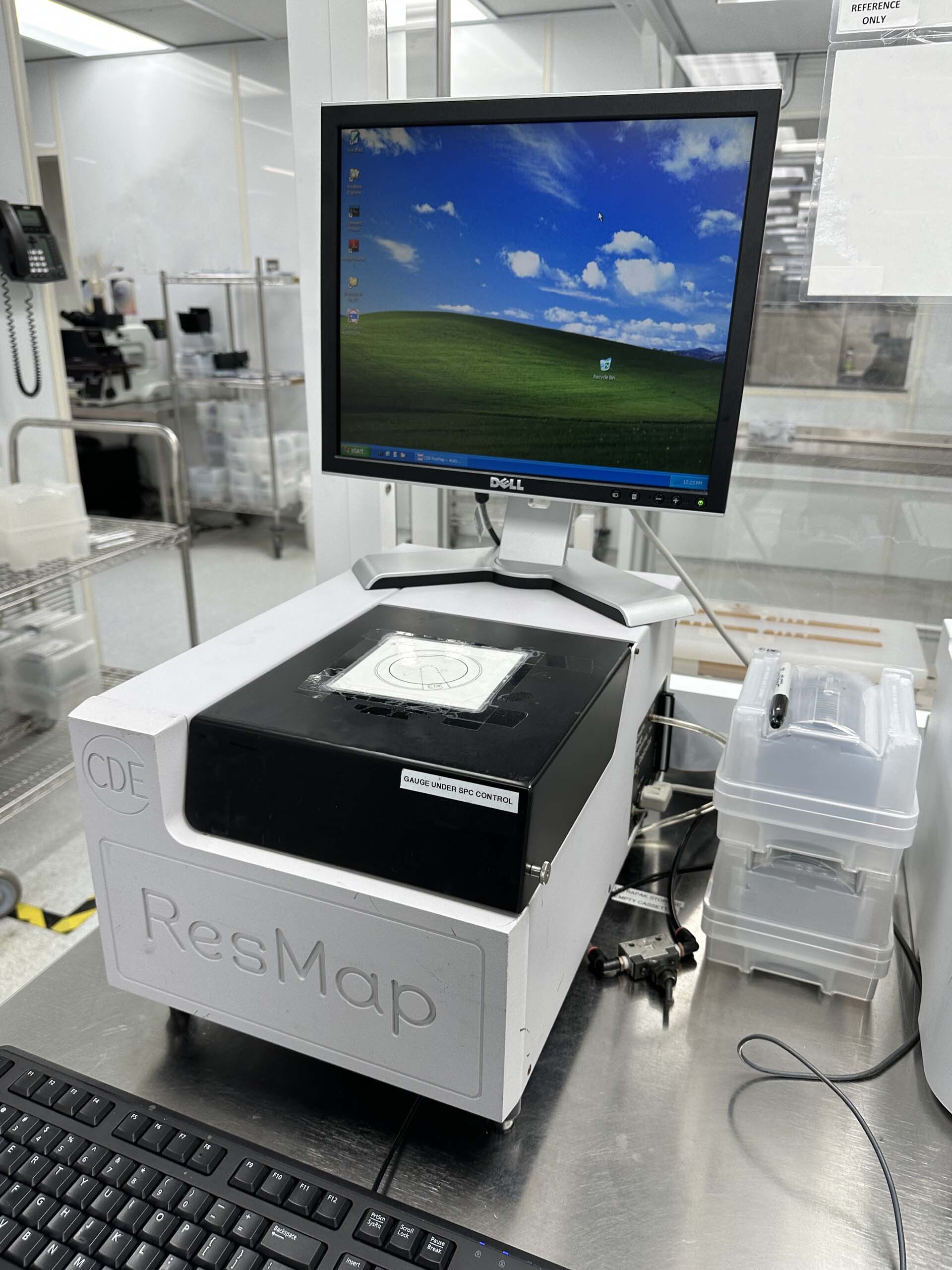
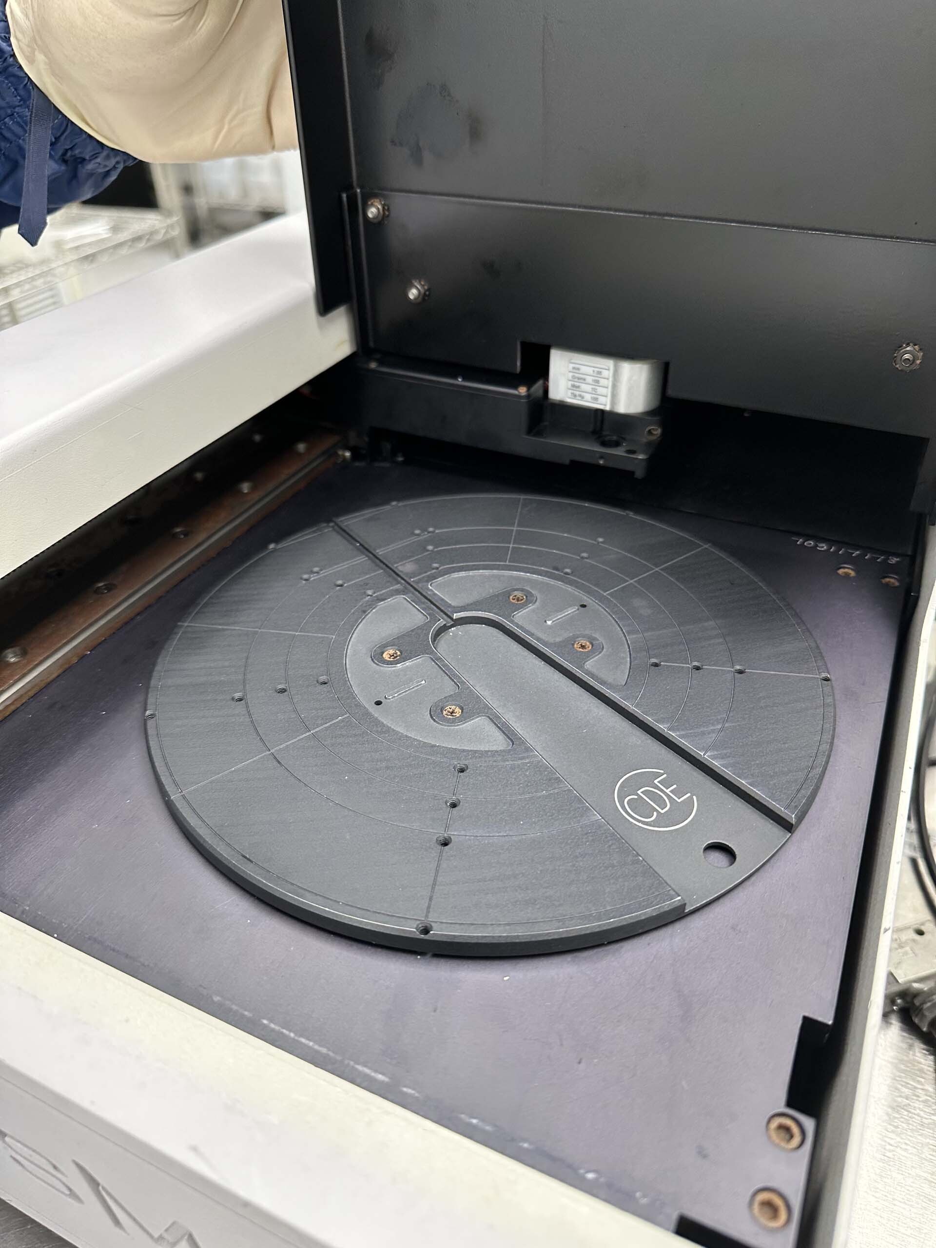
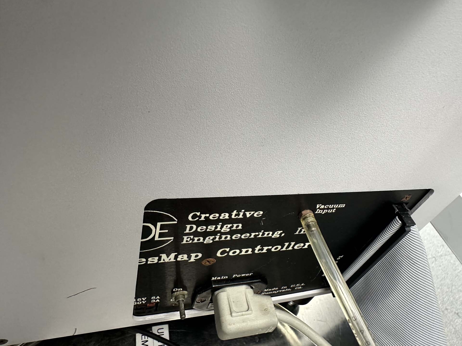
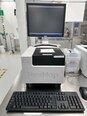
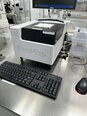
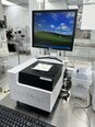
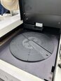
CDE RESMAP 178 is a wafer testing and metrology system designed to provide highly accurate measurements of a variety of structures on a wide range of process node sizes. This system is equipped with multiple optical and x-ray imaging technologies, including virtual microscope lithography (VML), x-ray diffraction (XRD), transmission electron microscopy (TEM), atomic force microscopy (AFM), and scanning electron microscopy (SEM). Each of these techniques allows for precise analysis of the structure of a wafer or substrate, enabling users to evaluate the accuracy of their designs or to locate defects or abnormalities. VML utilizes light-based imaging to create a three-dimensional image of the wafer that can detect changes in height and width across the surface, as well as very small features such as isolated lines or channels. This technology is useful in confirming patterns and verifying thickness more accurately than light microscopy. XRD is used to identify crystalline structure, thickness and composition. Through XRD, users can evaluate the quality of materials and their responsiveness to different process conditions. TEM and SEM are two electron-based imaging technologies that explore the surface of a substrate at an extremely high resolution. TEM helps identify the structure and morphology of a substrate, while SEM allows users to capture pictures of the surface at very high magnifications. AFM provides measurements of topography and surface properties, such as friction, adhesion, and elasticity. The all-in-one CDE RESMAP178 system combines numerous optical and x-ray imaging technologies and is designed to provide high-accuracy metrology solutions. It is a valuable tool for characterizing the structure of a wide variety of substrates, and is used in the manufacture of computer chips, solar cells, and other microtechnologies.
There are no reviews yet