Used CREAFORM HandySCAN 700 #293806559 for sale
URL successfully copied!

Tap to zoom
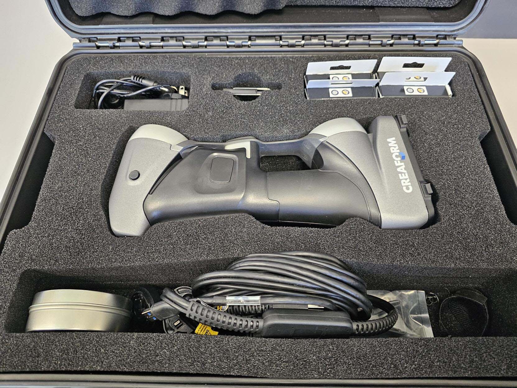

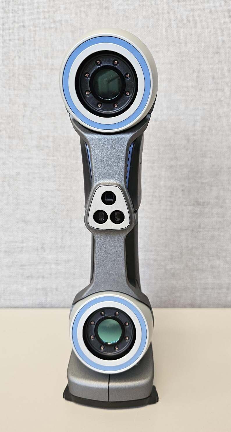
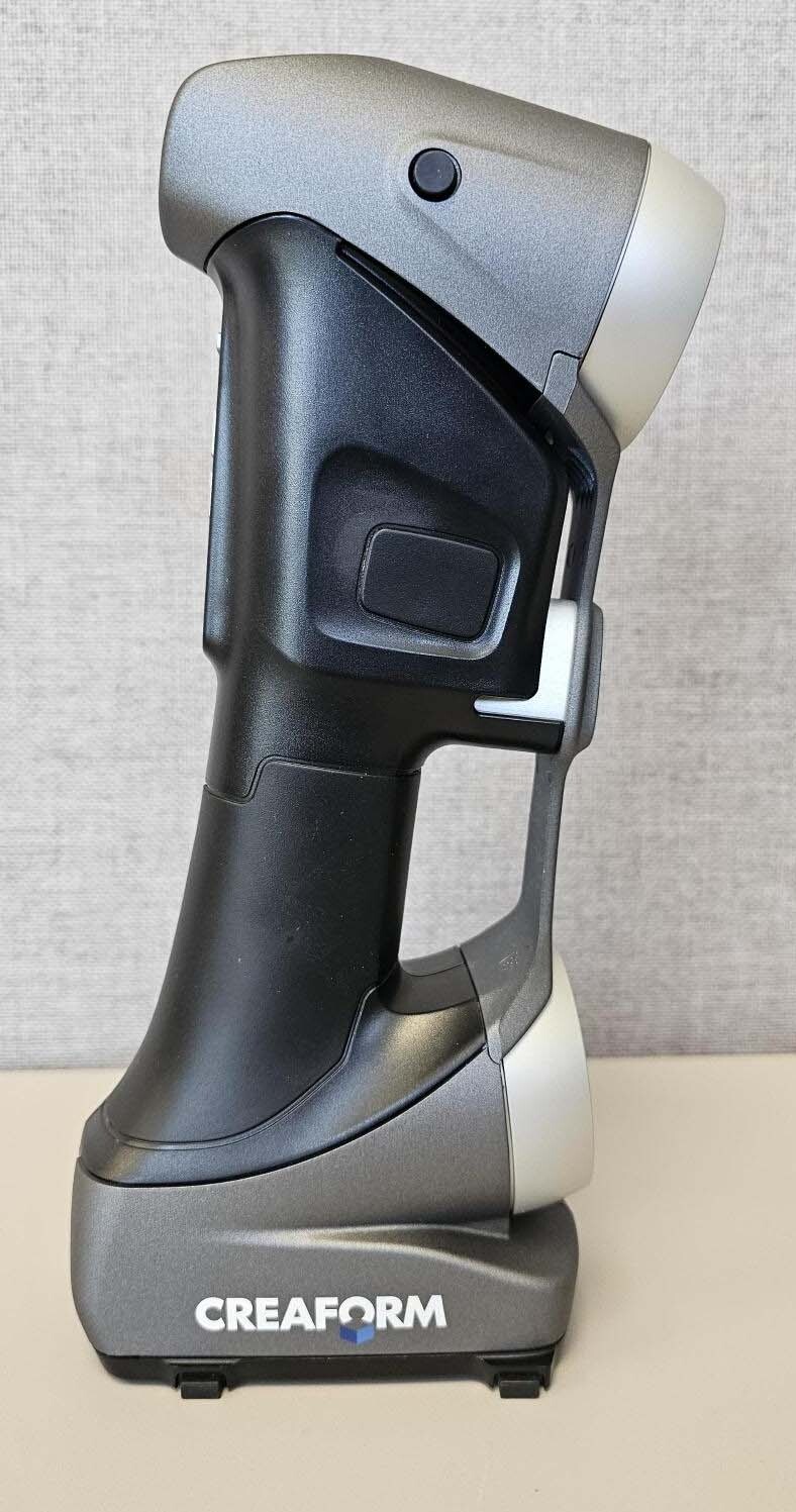
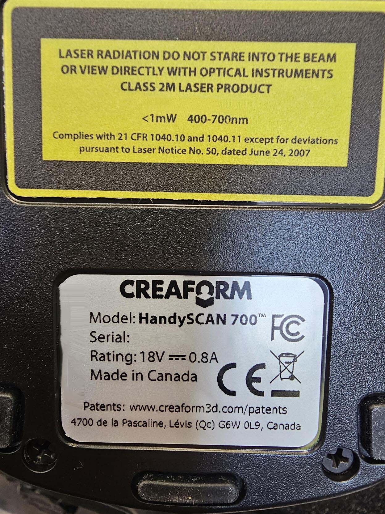
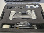
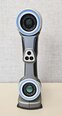
CREAFORM HandySCAN 700 is a cutting-edge metrology equipment designed specifically for wafer testing applications in the semiconductor industry. This advanced system integrates state-of-the-art technology to provide precise and reliable measurements of wafer characteristics with exceptional speed and accuracy. HandySCAN 700 is a portable and user-friendly tool that offers a high level of automation and efficiency in the inspection and metrology processes, making it an indispensable solution for quality control and process optimization in semiconductor manufacturing. At the core of CREAFORM HandySCAN 700 unit is a high-resolution 3D scanner that employs innovative laser scanning technology to capture detailed surface topography and geometric features of semiconductor wafers. The scanner is equipped with advanced sensors and optics that enable it to achieve sub-micron level accuracy in measurement, ensuring that even the most intricate and minute details of the wafer are captured with precision. This capability allows for comprehensive and thorough inspection of the wafer surface, facilitating the identification of defects, deviations, and anomalies that may impact the performance and quality of the semiconductor devices fabricated on the wafer. HandySCAN 700 machine utilizes sophisticated software algorithms and processing techniques to analyze the 3D data acquired from the wafer scans, generating comprehensive reports and visual representations of the wafer characteristics. The tool enables users to perform detailed metrology, including dimensional analysis, surface roughness measurements, flatness evaluations, and defect detection with exceptional accuracy and repeatability. The software interface is intuitive and user-friendly, allowing operators to easily configure measurement parameters, visualize the scan results, and generate customizable reports for further analysis and decision-making. One of the key features of CREAFORM HandySCAN 700 asset is its versatility and adaptability to a wide range of wafer sizes and materials commonly used in semiconductor fabrication. The model supports wafer diameters ranging from small-scale substrates to larger wafers up to 450mm, accommodating various wafer types such as silicon, gallium arsenide, and sapphire. This flexibility makes HandySCAN 700 an ideal solution for wafer testing and metrology in different semiconductor manufacturing applications, including integrated circuit fabrication, MEMS production, and optoelectronic device manufacturing. Furthermore, CREAFORM HandySCAN 700 equipment is designed for portability and ease of use, allowing users to perform on-site measurements and inspections directly in the fabrication facility or cleanroom environment. The compact and lightweight design of the system enables operators to move it easily between workstations and access hard-to-reach areas of the wafer for thorough scanning and analysis. This portability enhances productivity and efficiency in wafer testing processes, enabling real-time feedback and quality control during semiconductor production. In conclusion, HandySCAN 700 is a state-of-the-art metrology unit that offers unparalleled capabilities for wafer testing and inspection in the semiconductor industry. With its advanced 3D scanning technology, high accuracy measurements, versatile compatibility, and user-friendly interface, CREAFORM HandySCAN 700 machine provides semiconductor manufacturers with a powerful tool for quality assurance, process optimization, and product development in wafer fabrication.
There are no reviews yet