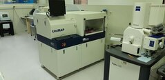
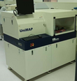
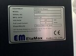
Used EM ETAMAX UniMAP #293674206 for sale
URL successfully copied!

Tap to zoom
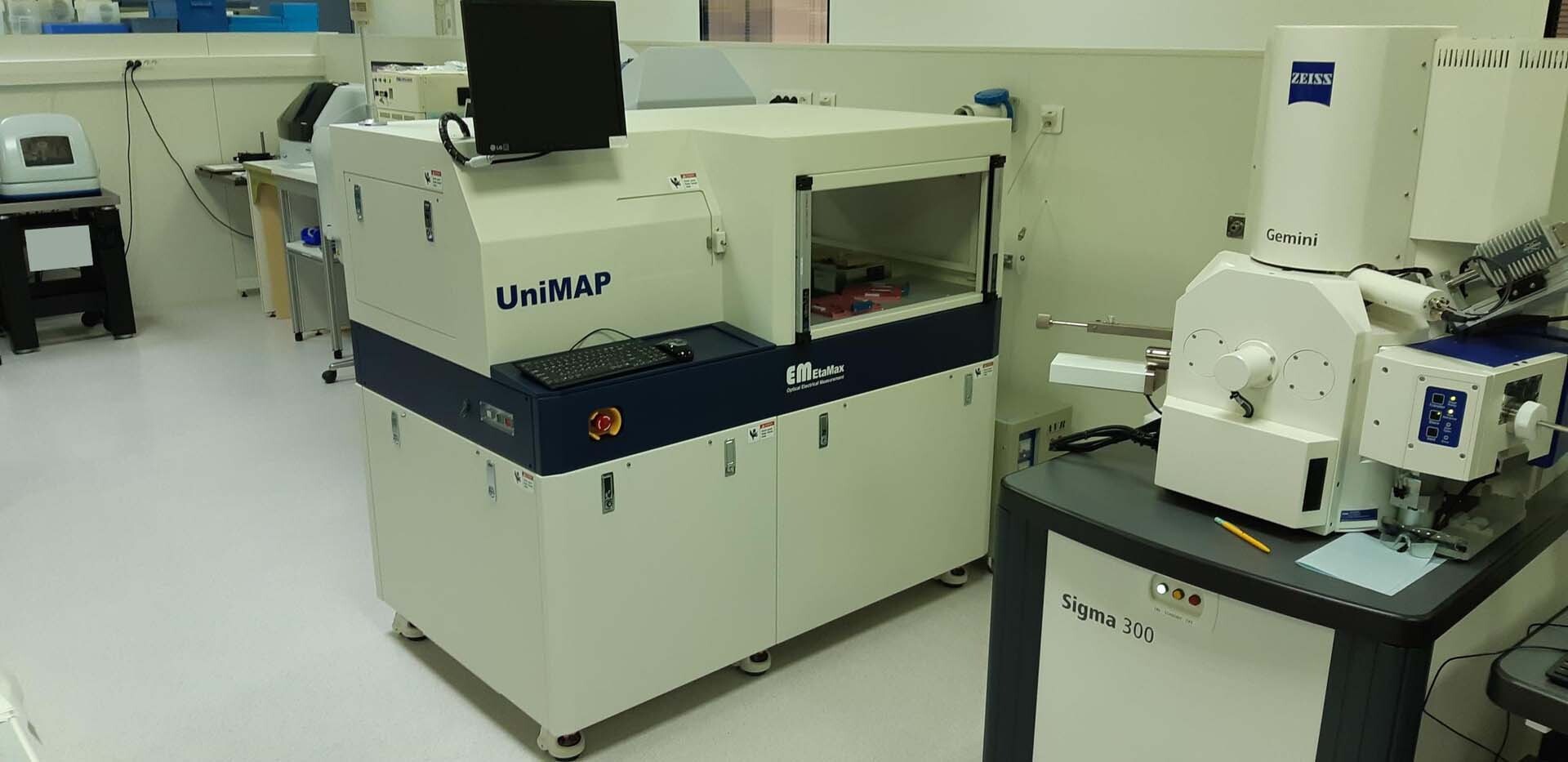

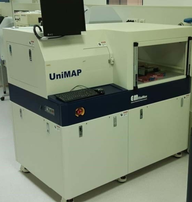
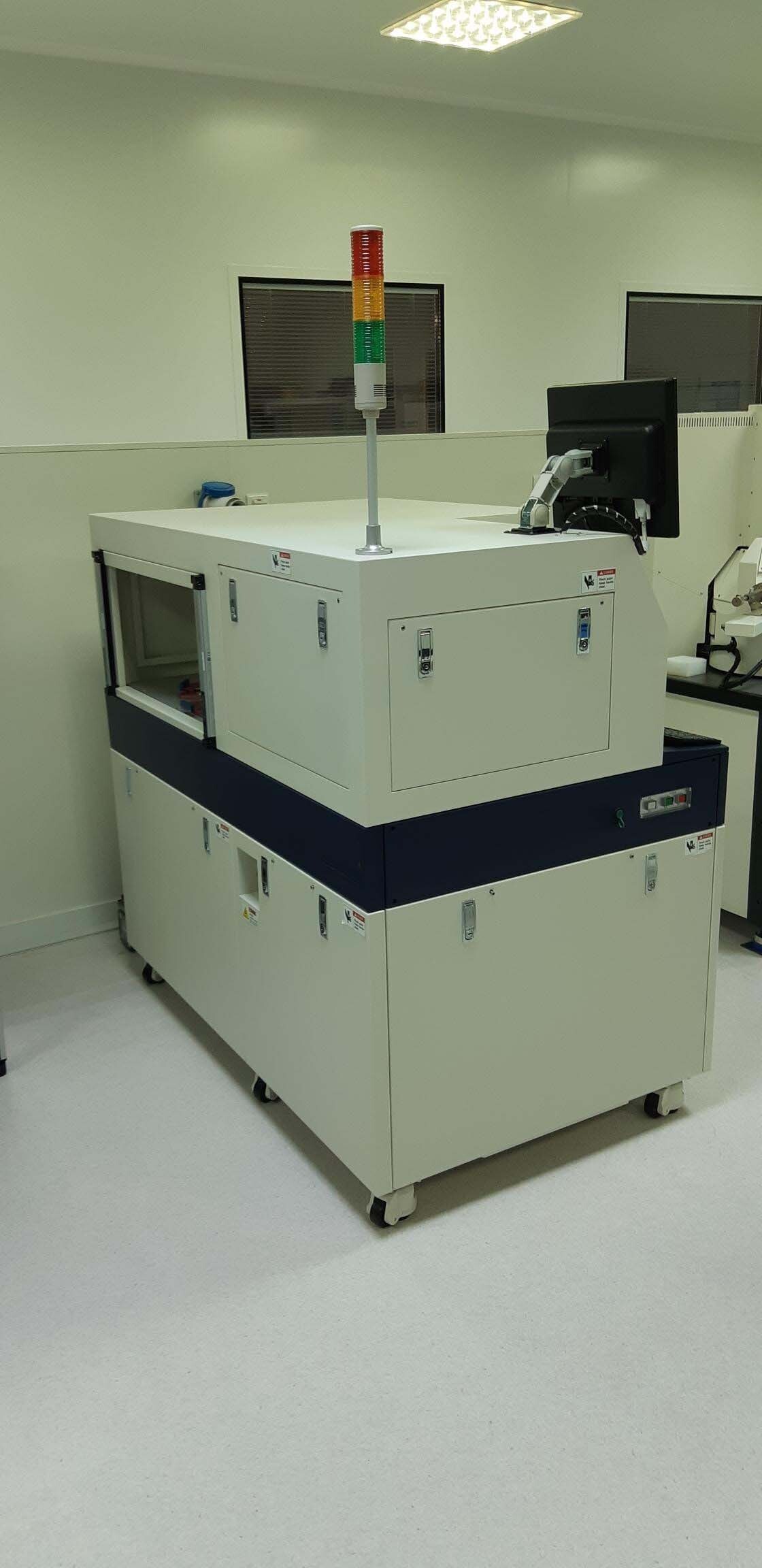
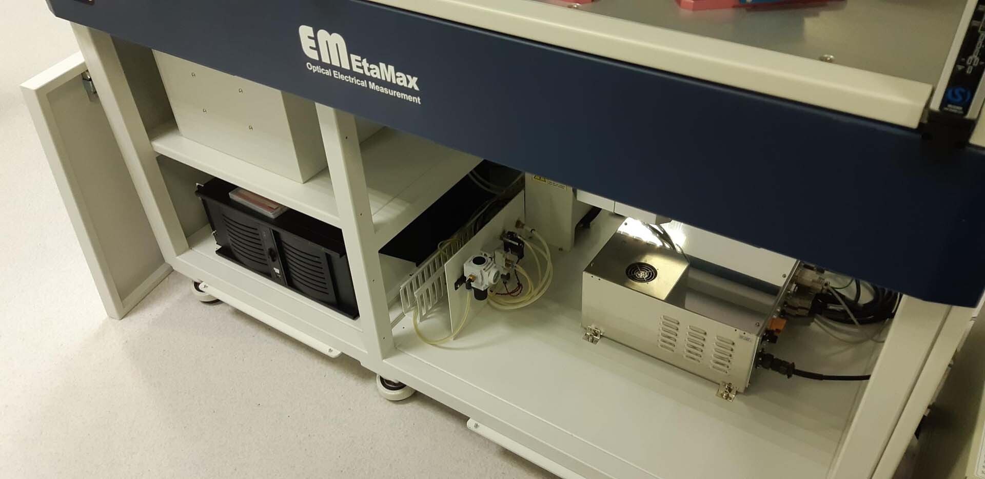
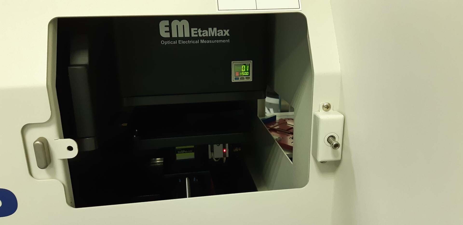
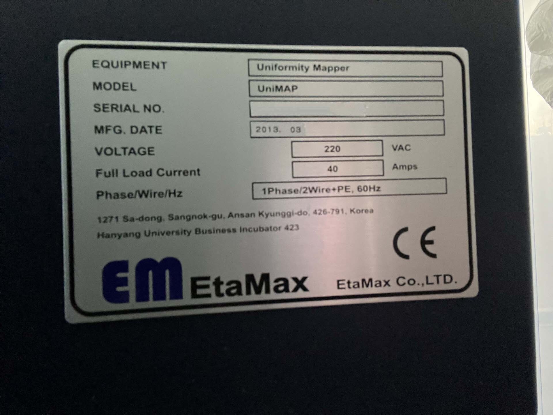
ID: 293674206
Vintage: 2013
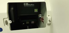
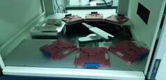
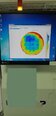
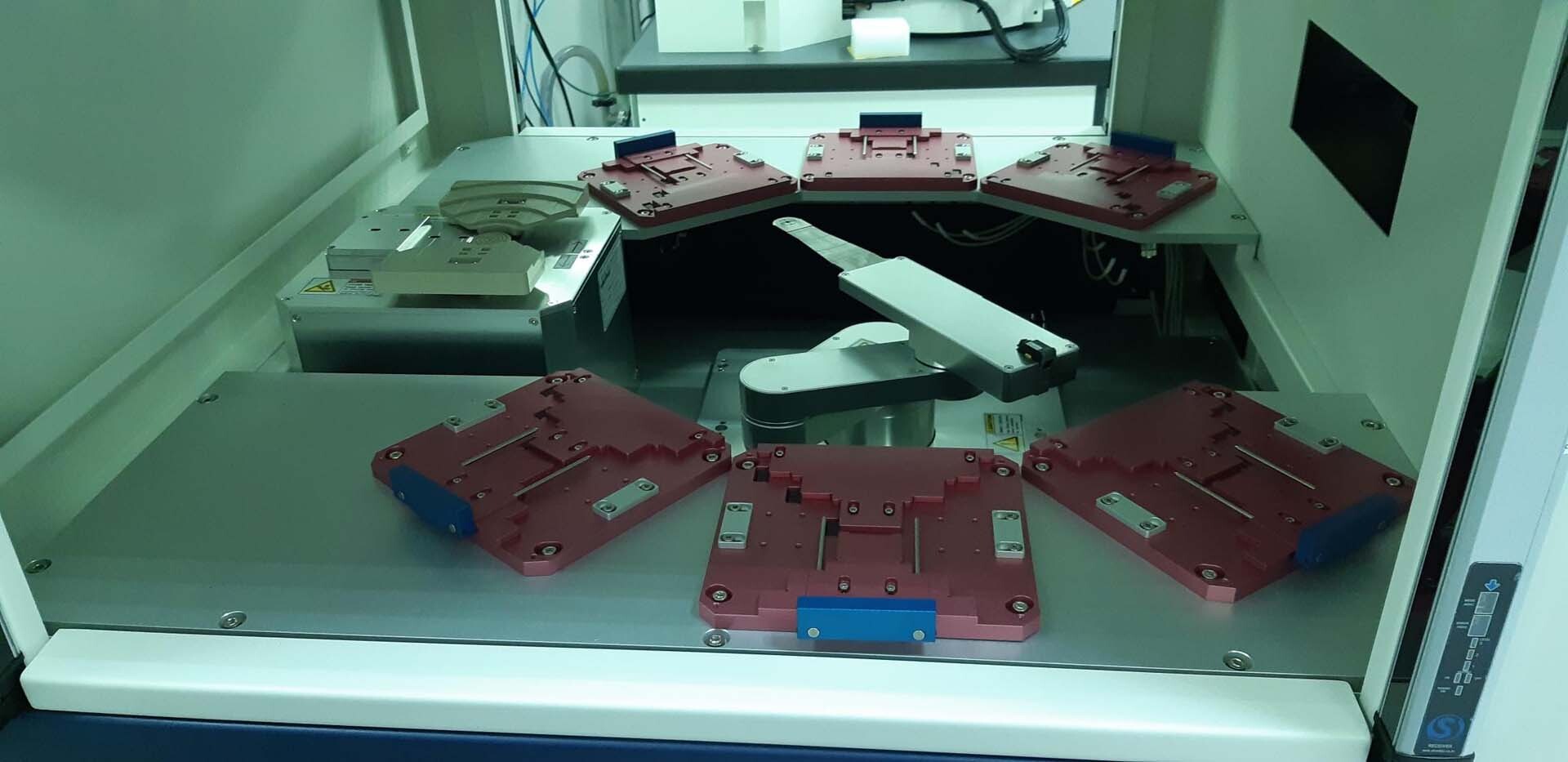
Automatic reflectivity mapping system
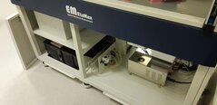
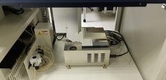
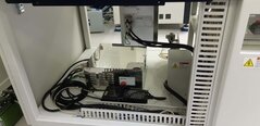
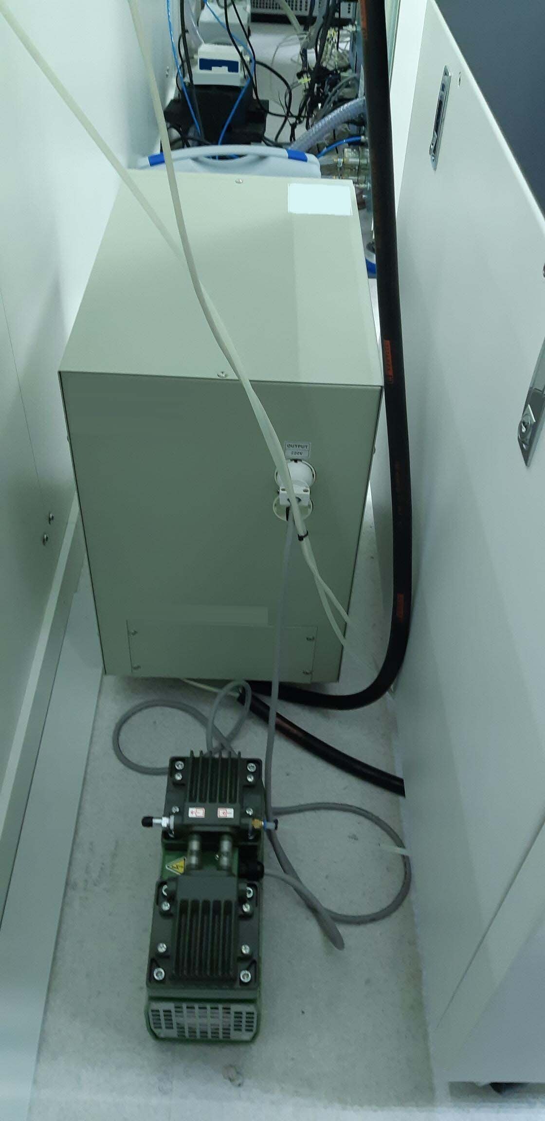
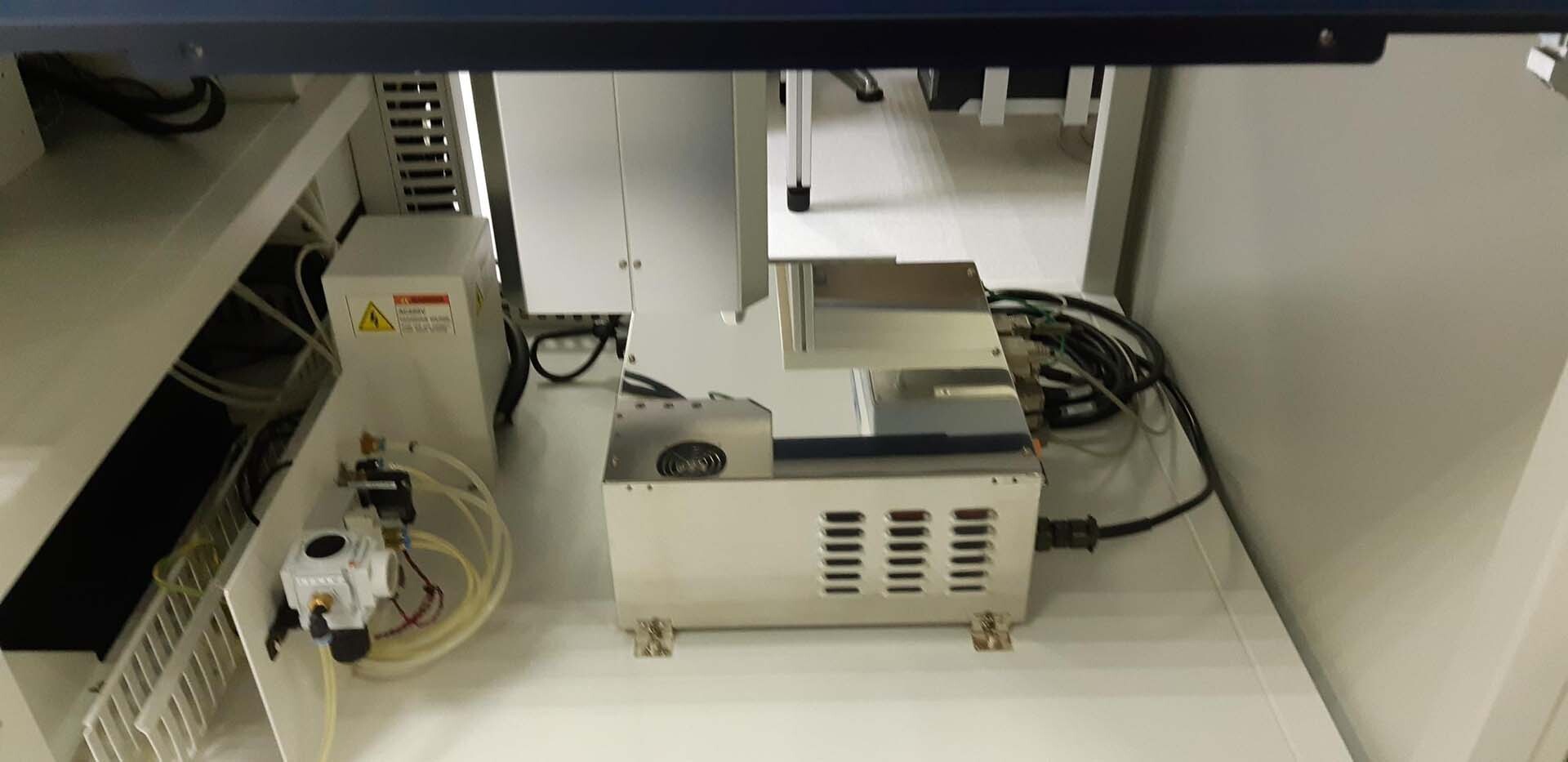
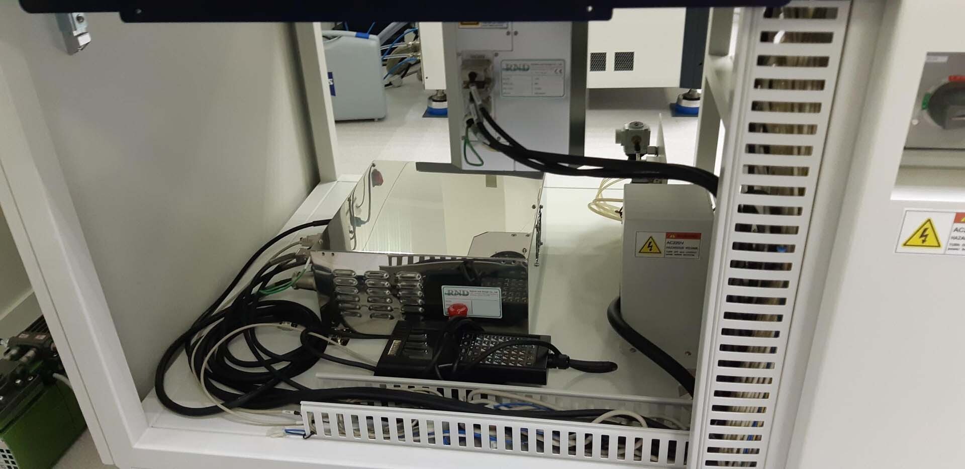
With transformer for EU voltage, 230V
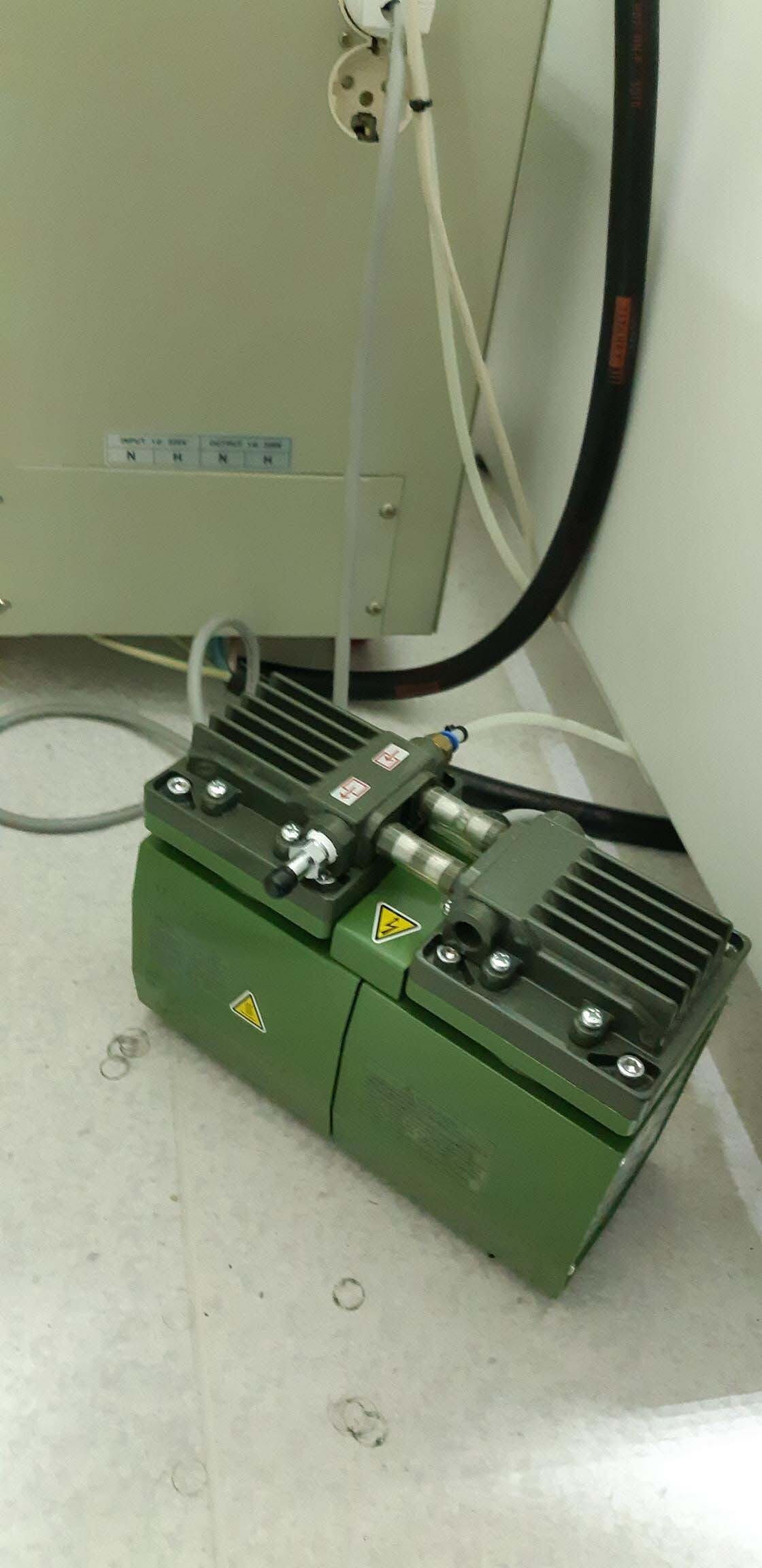
ULVAC Vacuum pump for robot
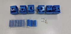
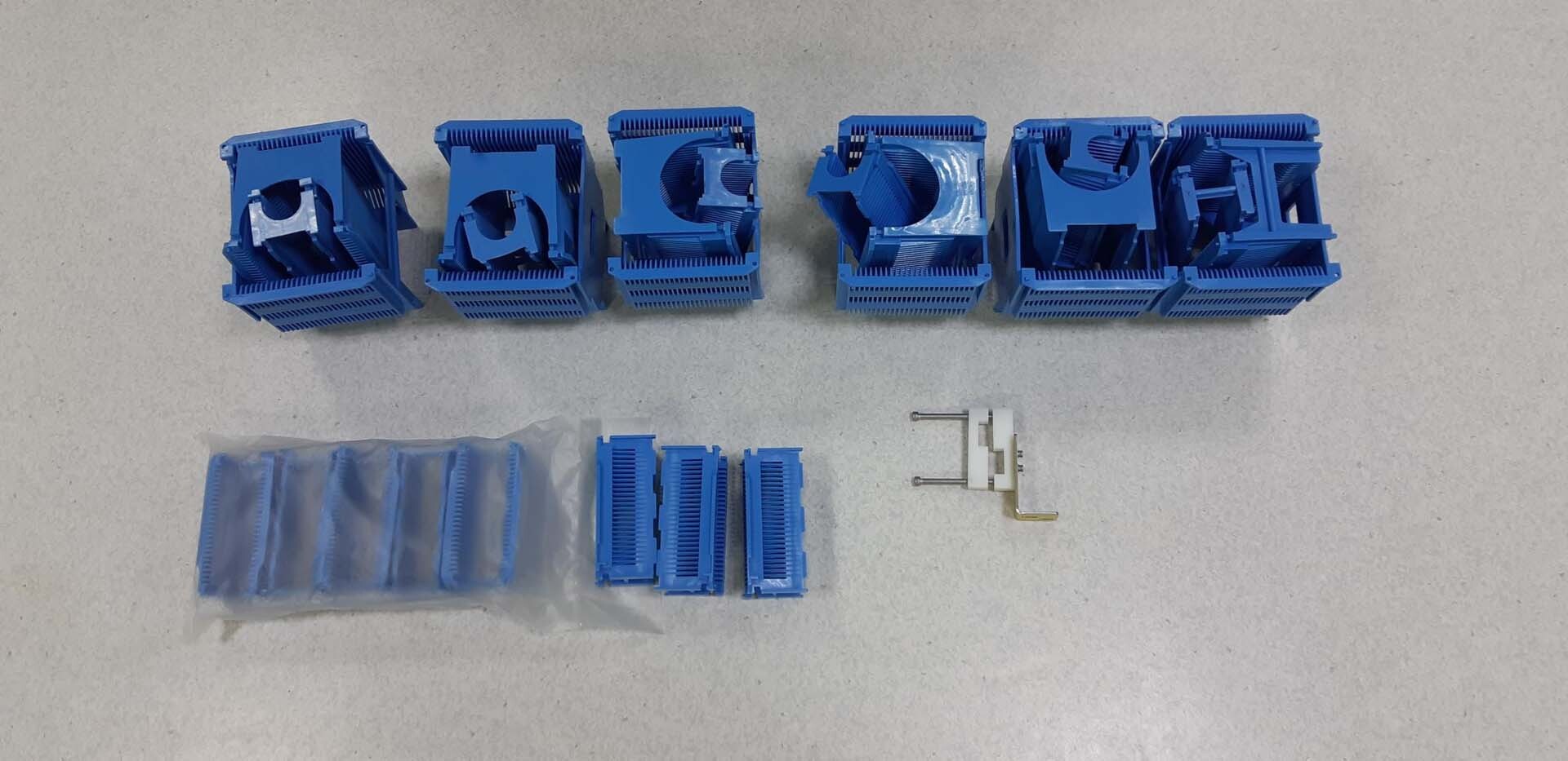
(14) Cassettes, 2"
(6) Cassettes, 4"
(6) Cassettes, 6"
X-Y Stage: AC Servo control
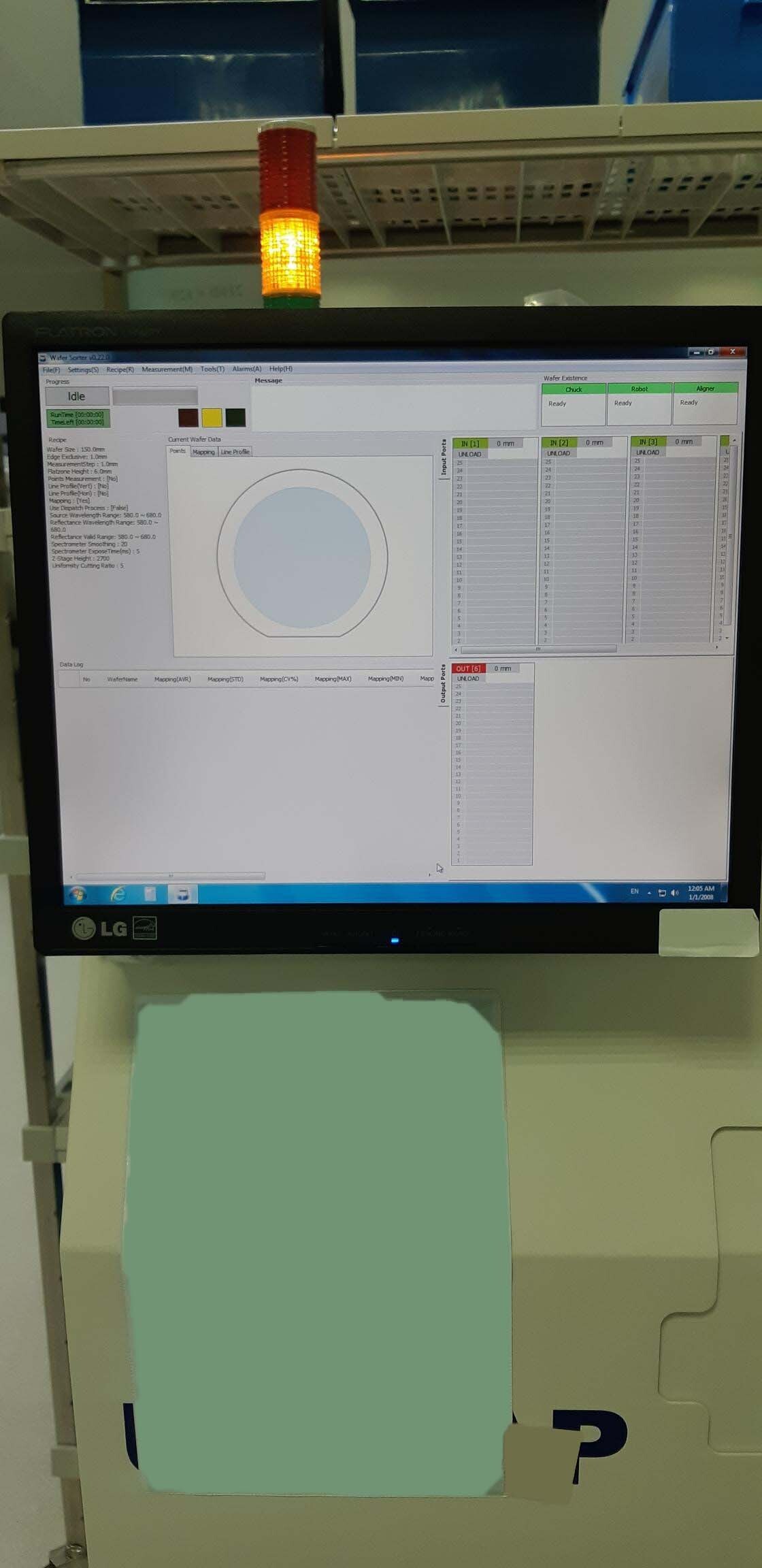
Cassette holder: 2"-6"
Operating cassette size: 2"-6"
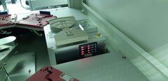
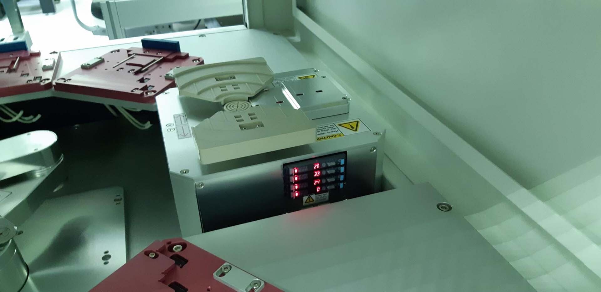
Robot type: Auto loader
Flat zone finder
Z-Stage adjustment
Light source:
White LED: Reflectance measurement
LED Intensity monitoring: One sensor
Spectrometer:
3636 Pixels
Wavelength range: 420 nm, span: 380-800 nm
Hardware pixel resolution : 0.13 nm/pixel
Optic slit: 50 µm
USB Control
Filters and lens
Measurements:
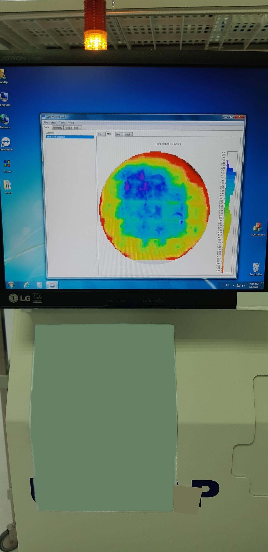
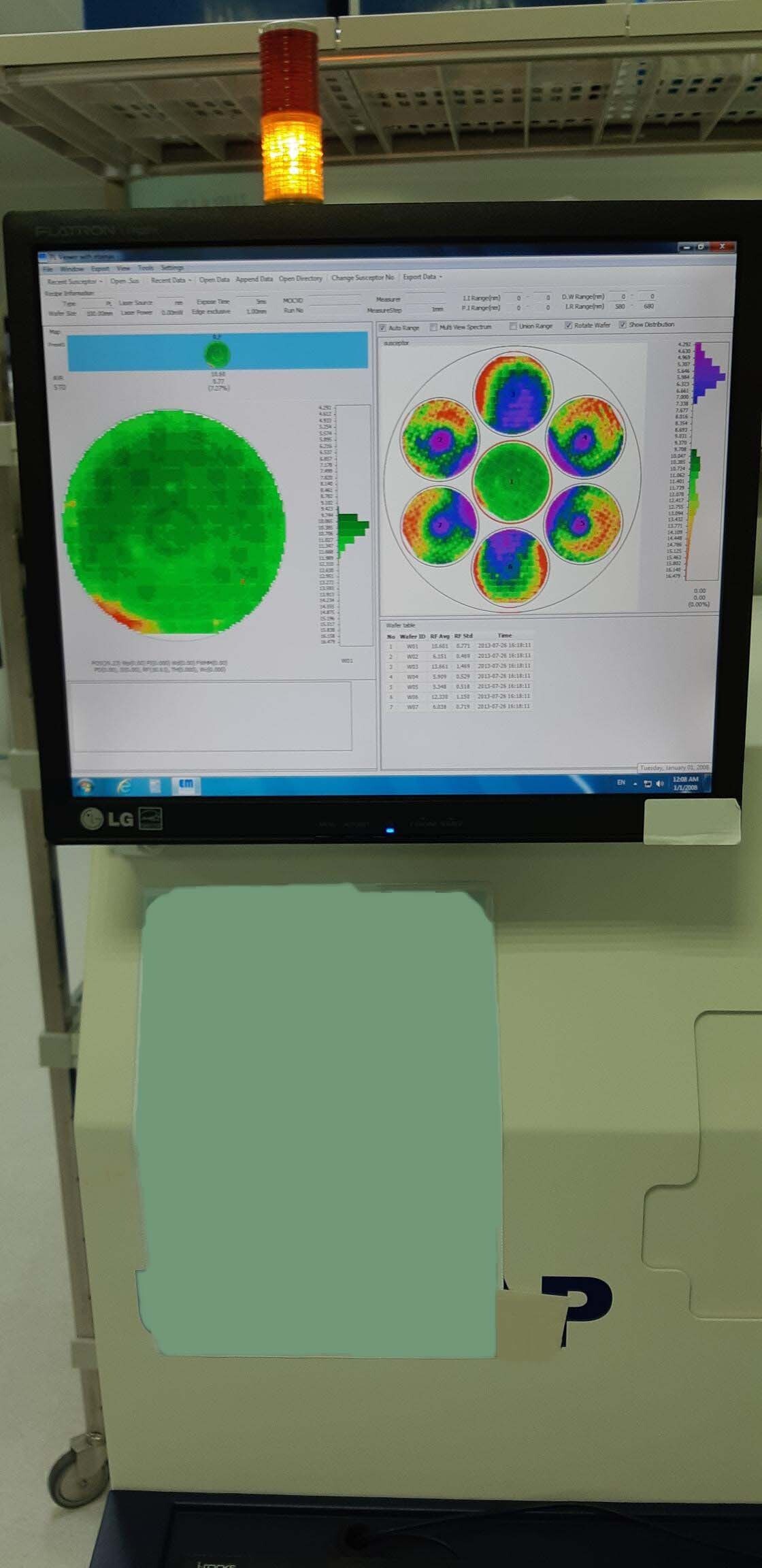
Wafer surface uniformity
Reflectance by spectrometer
Calculated by maximum - minimum / Maximum + minimum
Calculated by standard deviation
Minimum and maximum value of reflectance
Data acquisition PC:
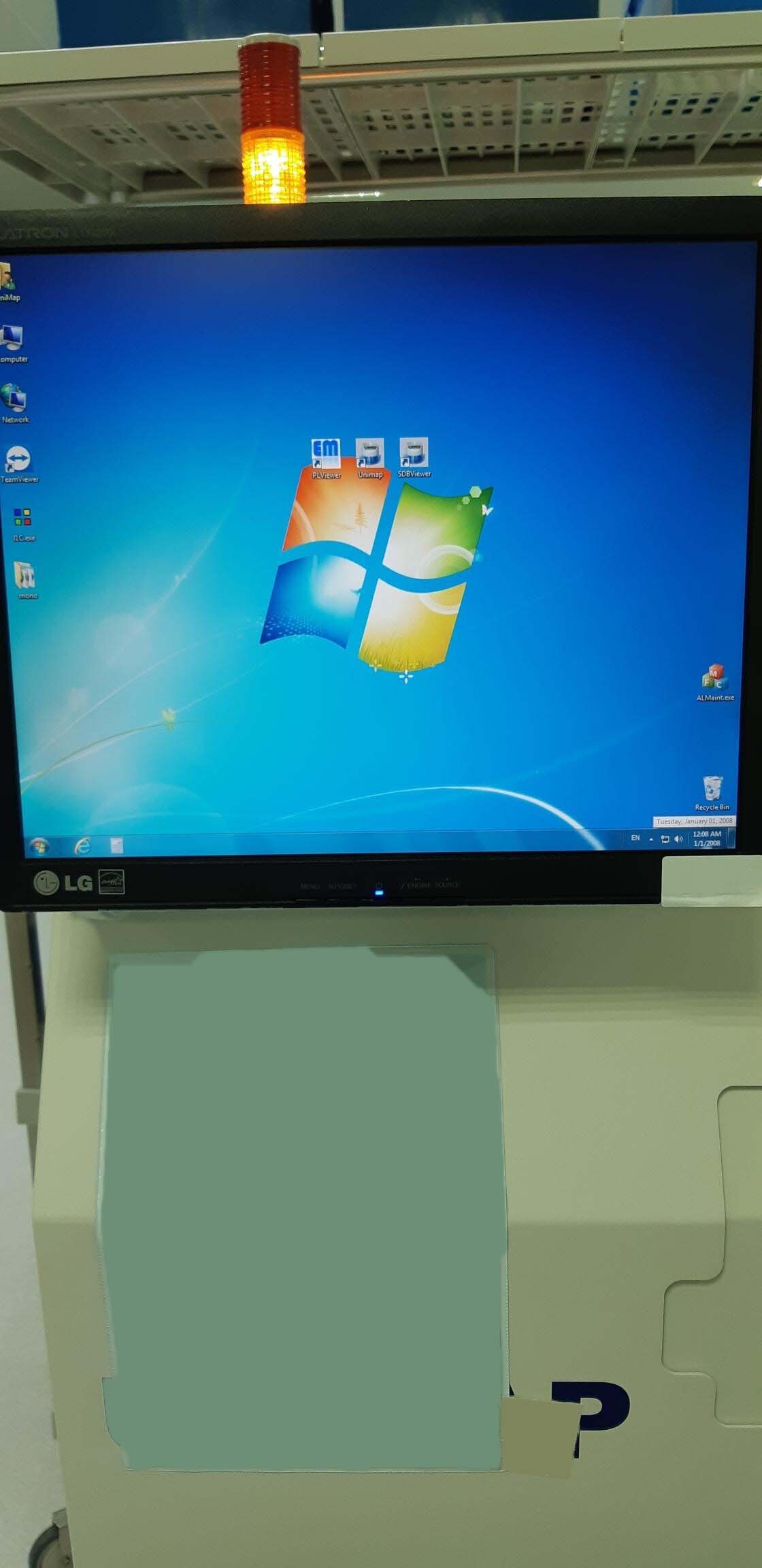
Operating system: Windows 7
LCD Monitor, 17
Sorting function:
PSS Uniformity / Reflectance mapping
Power supply: 220 V, 30 A, 3-Wires
CDA: 0.2 ~ 0.4 Mpa
2013 vintage.
EM ETAMAX UniMAP is a cutting-edge wafer testing and metrology equipment designed to provide comprehensive analysis and characterization of semiconductor wafers. This system is equipped with advanced electromagnetic (EM) testing capabilities and utilizes the latest technologies to deliver precise and reliable results for semiconductor manufacturing processes. UniMAP unit offers a wide range of testing and metrology functions essential for ensuring the quality and performance of semiconductor wafers. It is capable of measuring various electromagnetic properties of wafers, including conductivity, permittivity, and dielectric constant. These measurements are crucial for evaluating the electrical and physical properties of semiconductor materials used in device fabrication. One of the key features of EM ETAMAX UniMAP machine is its high measurement accuracy and sensitivity. The tool uses advanced sensor technology and signal processing algorithms to achieve precise and reliable measurements, even in demanding semiconductor manufacturing environments. This ensures that semiconductor manufacturers can trust the data generated by the asset for critical decision-making processes. In addition to its electromagnetic testing capabilities, UniMAP model also offers comprehensive metrology functions for characterizing wafer properties. The equipment can perform topography analysis, thickness measurements, and defect detection on wafers with high precision and throughput. This helps semiconductor manufacturers identify any issues with the wafers early in the production process and make necessary adjustments to improve yield and product quality. Another important aspect of EM ETAMAX UniMAP system is its versatility and flexibility. The unit is designed to accommodate various wafer sizes and types commonly used in semiconductor manufacturing, making it suitable for a wide range of applications. Whether manufacturers are working with silicon wafers, compound semiconductors, or other materials, UniMAP machine can provide accurate and reliable data for process optimization. Furthermore, EM ETAMAX UniMAP tool is equipped with user-friendly software interfaces and intuitive controls, allowing operators to easily set up tests, analyze data, and generate reports. The asset also supports automation and integration with other manufacturing equipment, streamlining the testing and metrology processes for improved efficiency and productivity. Overall, UniMAP model is a powerful tool for semiconductor manufacturers looking to enhance their wafer testing and metrology capabilities. With its advanced EM testing technology, comprehensive metrology functions, and user-friendly design, the equipment enables manufacturers to achieve higher levels of quality control, process optimization, and product performance in semiconductor production.
There are no reviews yet