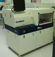
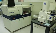
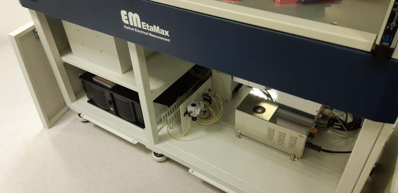
Used EM ETAMAX UniMAP #9360878 for sale
URL successfully copied!
Tap to zoom


























ID: 9360878
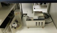
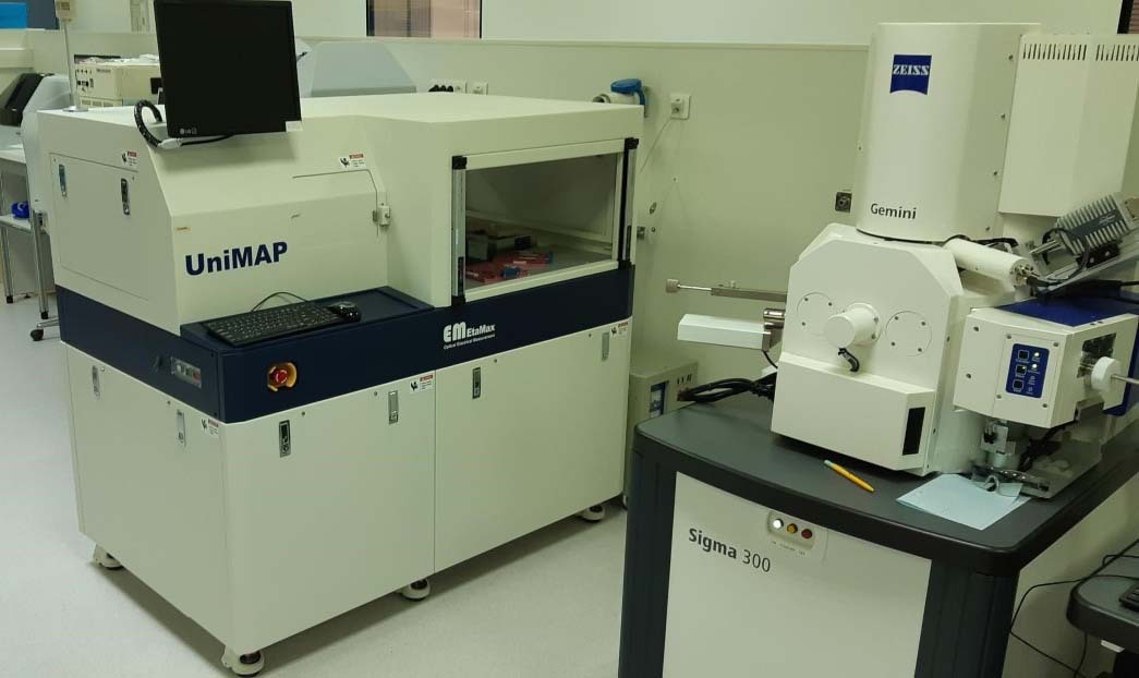
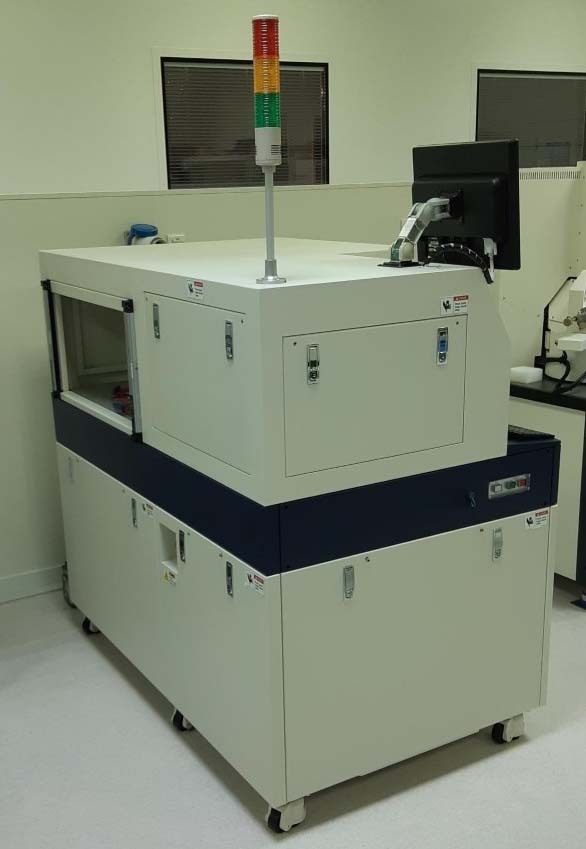
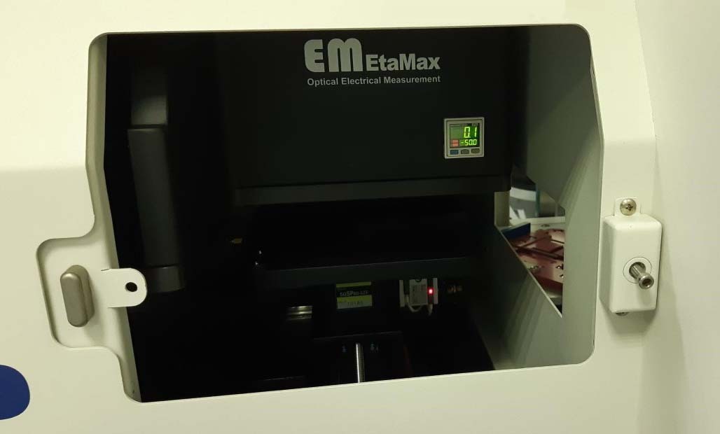
Automatic reflectivity mapping system
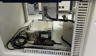
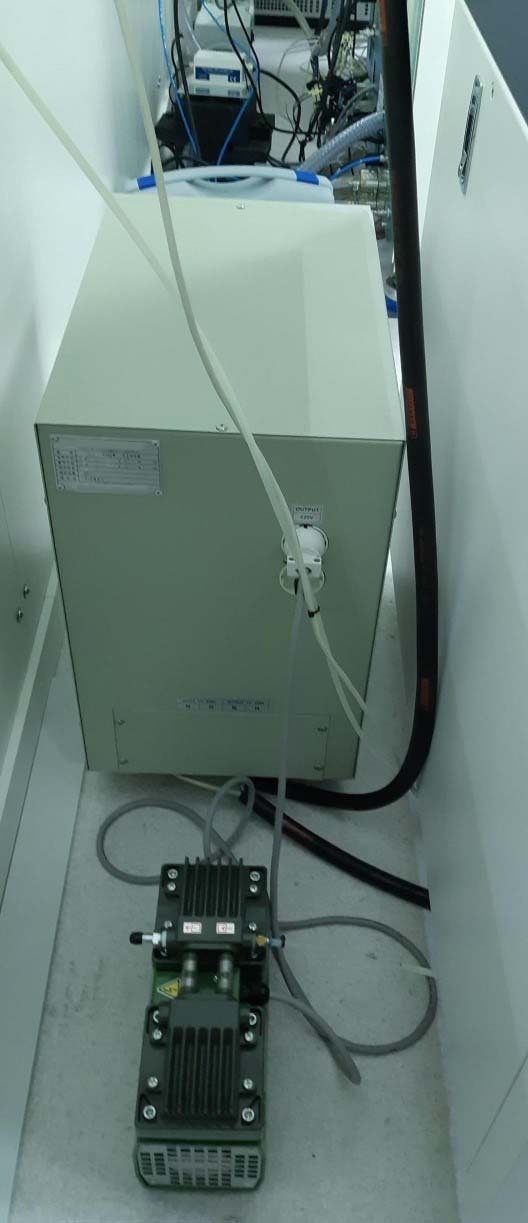
With transformer for EU voltage, 230V
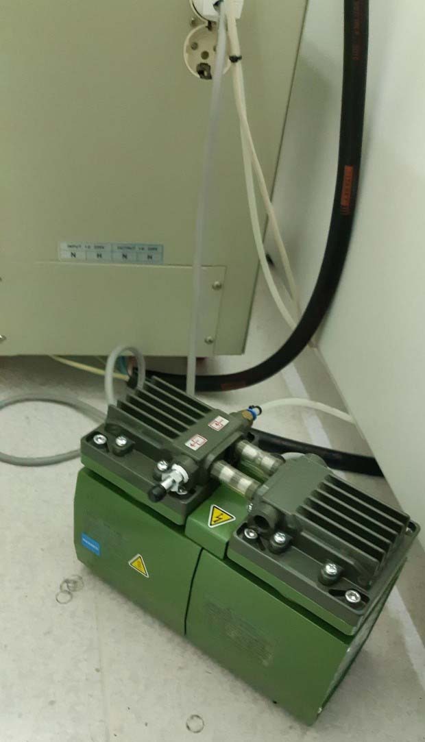
ULVAC Vacuum pump for robot
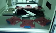
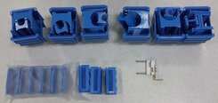
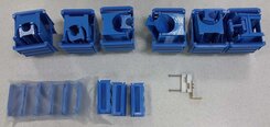
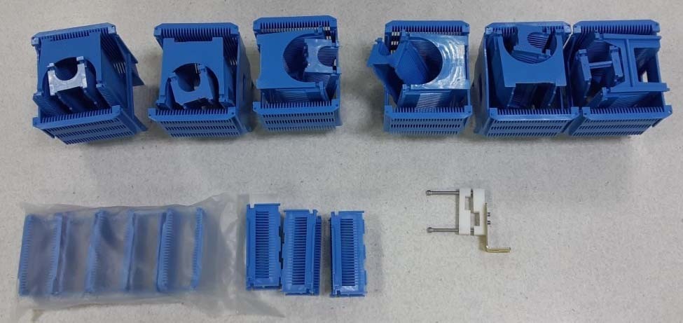
(14) Cassettes, 2"
(6) Cassettes, 4"
(6) Cassettes, 6"
Main frame:
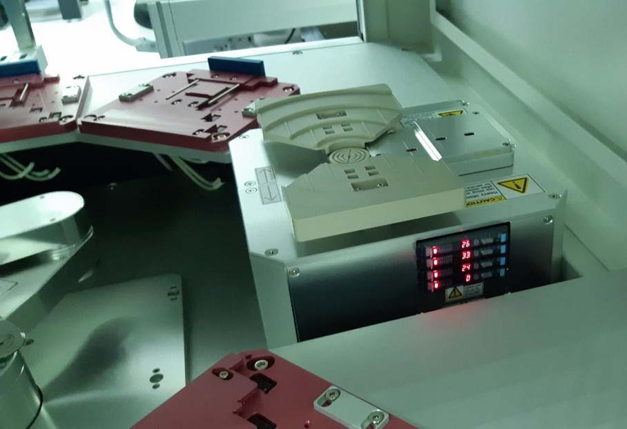
X-Y Stage: AC Servo control
Cassette holder: 2"-6"
Operating cassette size: 2"-6"
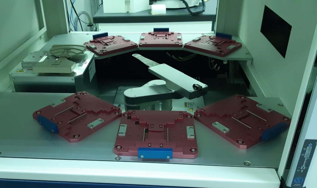
Robot type: Auto loader
Flat zone finder
Z-Stage adjustment
Light source:
White LED: Reflectance measurement
LED Intensity monitoring: One sensor
Spectrometer:
3636 Pixels
Wavelength range: 420 nm, span: 380-800 nm
Hardware pixel resolution : 0.13 nm/pixel
Optic slit: 50 µm
USB Control
Filters and lens
Measurements:
Wafer surface uniformity
Reflectance by spectrometer
Calculated by maximum - minimum / Maximum + minimum
Calculated by standard deviation
Minimum and maximum value of reflectance
Data acquisition PC:
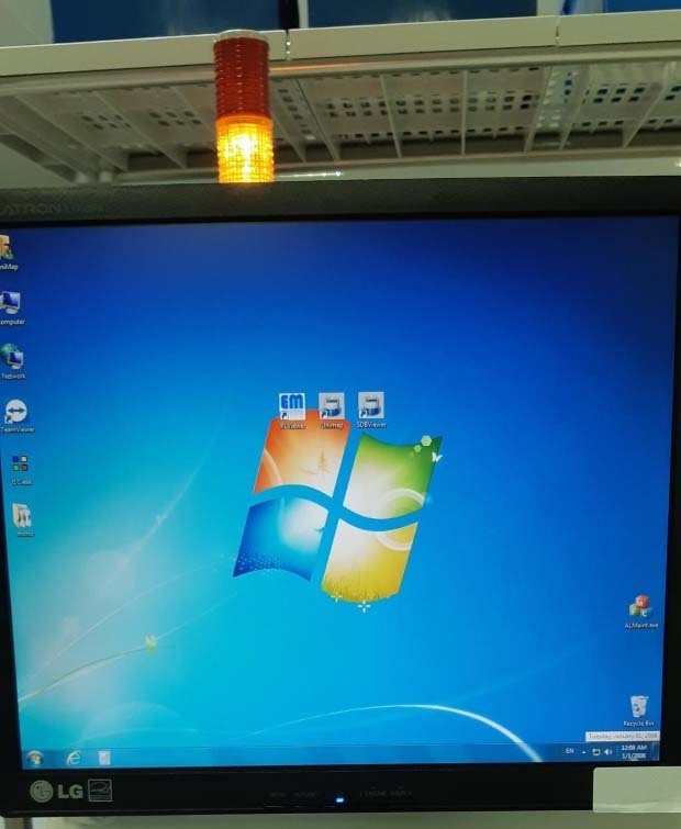
Operating system: Windows 7
LCD Monitor, 17
Sorting function:
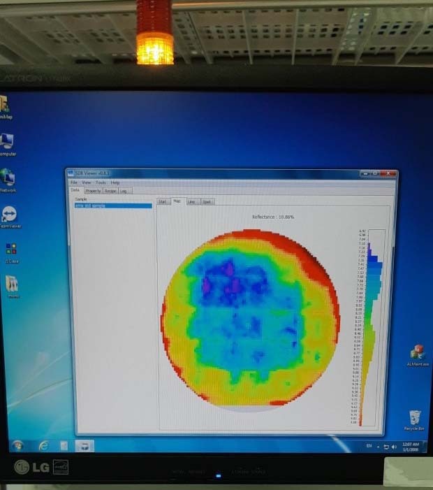
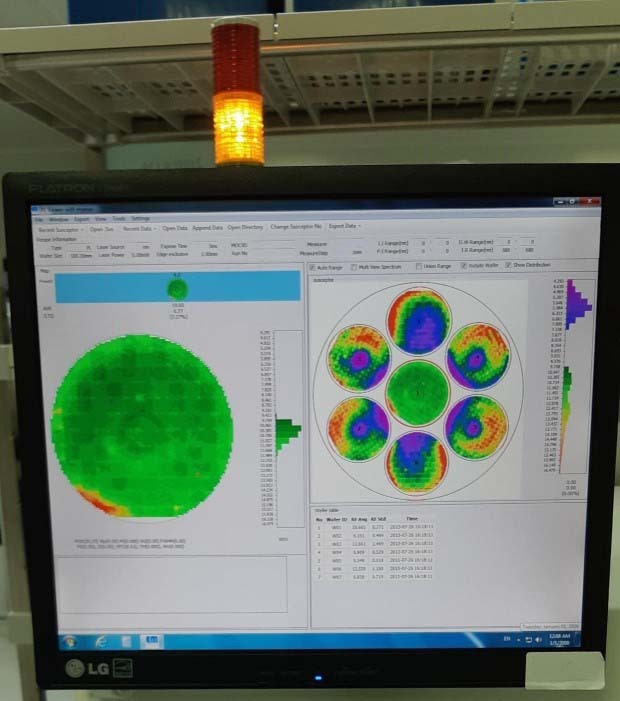
PSS Uniformity / Reflectance mapping
Power supply: 220 V, 30 A, 3-Wires
CDA: 0.2 ~ 0.4 Mpa.
The ETAMAX EM ETAMAX UniMAP equipment is a wafer testing and metrology tool that provides a comprehensive solution for measuring the electrical and physical properties of semiconductor wafers and chips. This system covers all aspects of wafer testing, from design to analysis, ensuring that the wafer meets all industry standards and specifications. ETAMAX UniMAP consists of three core modules: process control, test instrumentation, and metrology. Process control uses AutoCell technology to provide precise and accurate control over the process parameters and test conditions. This helps to ensure that the wafers are produced to customer-specified specs. Test instrumentation includes a range of specialized automated tools that are used to measure different electrical properties of the wafer, such as resistance, capacitance, and leakage current. Metrology is used to measure physical wafer parameters, such as thickness and curvature. It is also used to detect defects that can affect the performance of the wafer. When testing wafers with ETAMAX EM ETAMAX UniMAP, users can set up a test sequence to measure the specific characteristics they wish to assess. The unit offers a range of methods for collecting data, including contact imaging, force, and thermal scanning. The machine can also be used to analyze data, compare results to past specifications, and make recommendations for corrective actions, if needed. ETAMAX UniMAP is one of the most advanced wafer testing and metrology systems in the industry, offering users unsurpassed accuracy and a reliable platform for wafer assessment. The tool is extremely efficient, making it an ideal choice for wafer testing in production lines. Its user-friendly interface and intuitive control panel make it user-friendly and easy to use. Moreover, its software runs on PCs, eliminating the need for dedicated hardware. Overall, ETAMAX EM ETAMAX UniMAP is a powerful, reliable, and cost-effective wafer testing and metrology asset, providing users with comprehensive solutions for measuring and assessing semiconductor wafers and chips. Its advanced features and comprehensive capabilities make it a reliable choice for accurate and reliable wafer processing.
There are no reviews yet
