Used FILMETRICS F10-RT-UV #293768760 for sale
URL successfully copied!
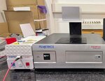
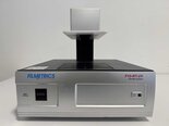
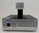
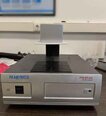
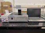
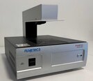
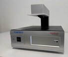
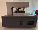
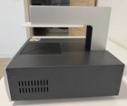
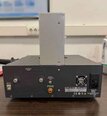
Tap to zoom

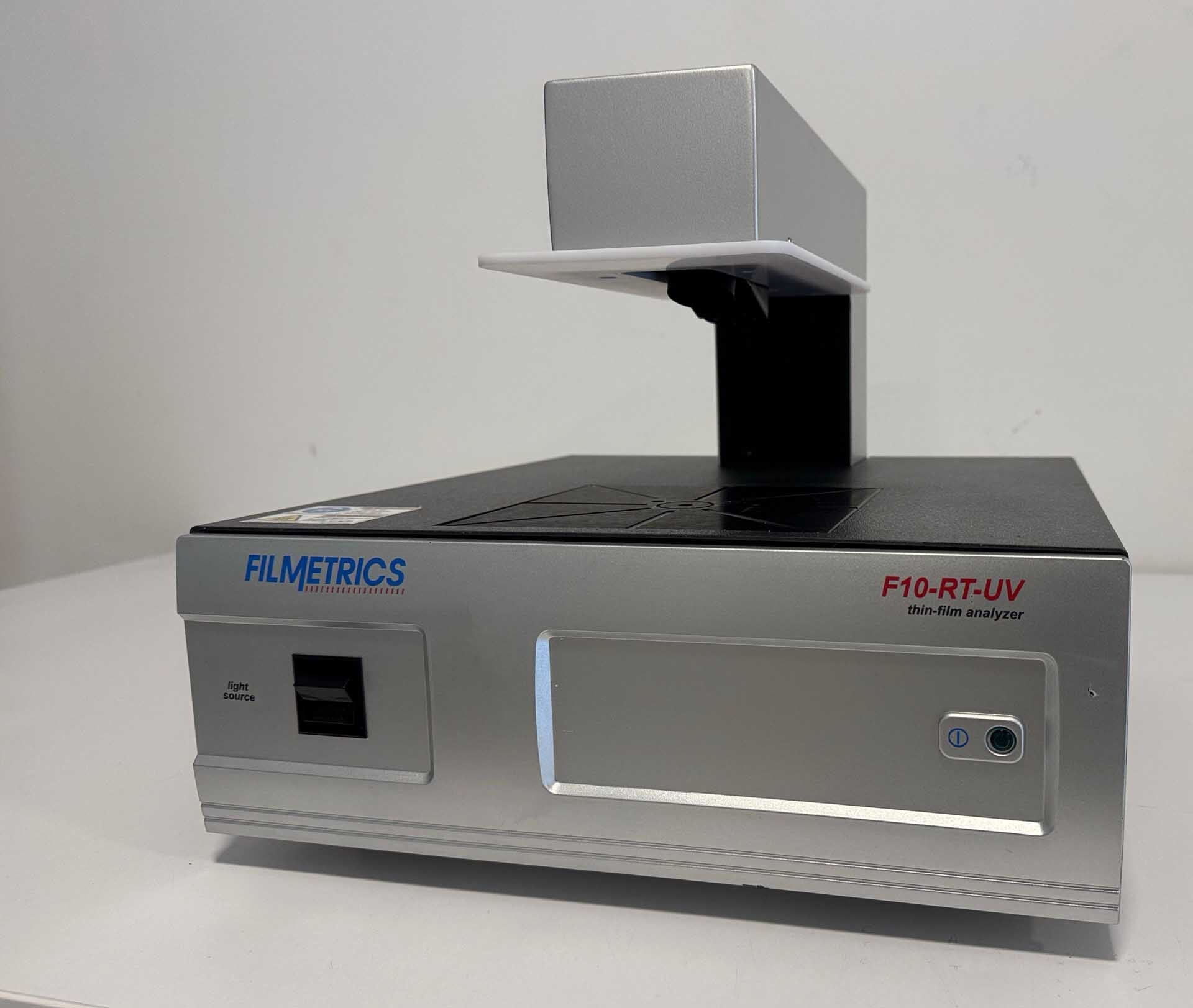
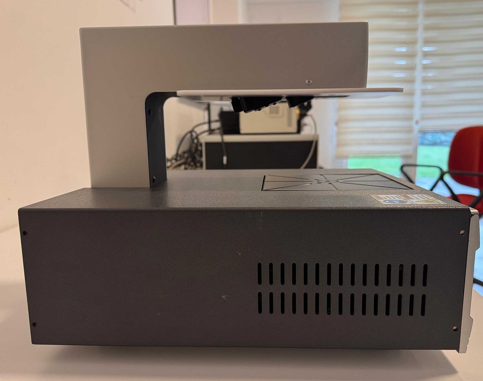
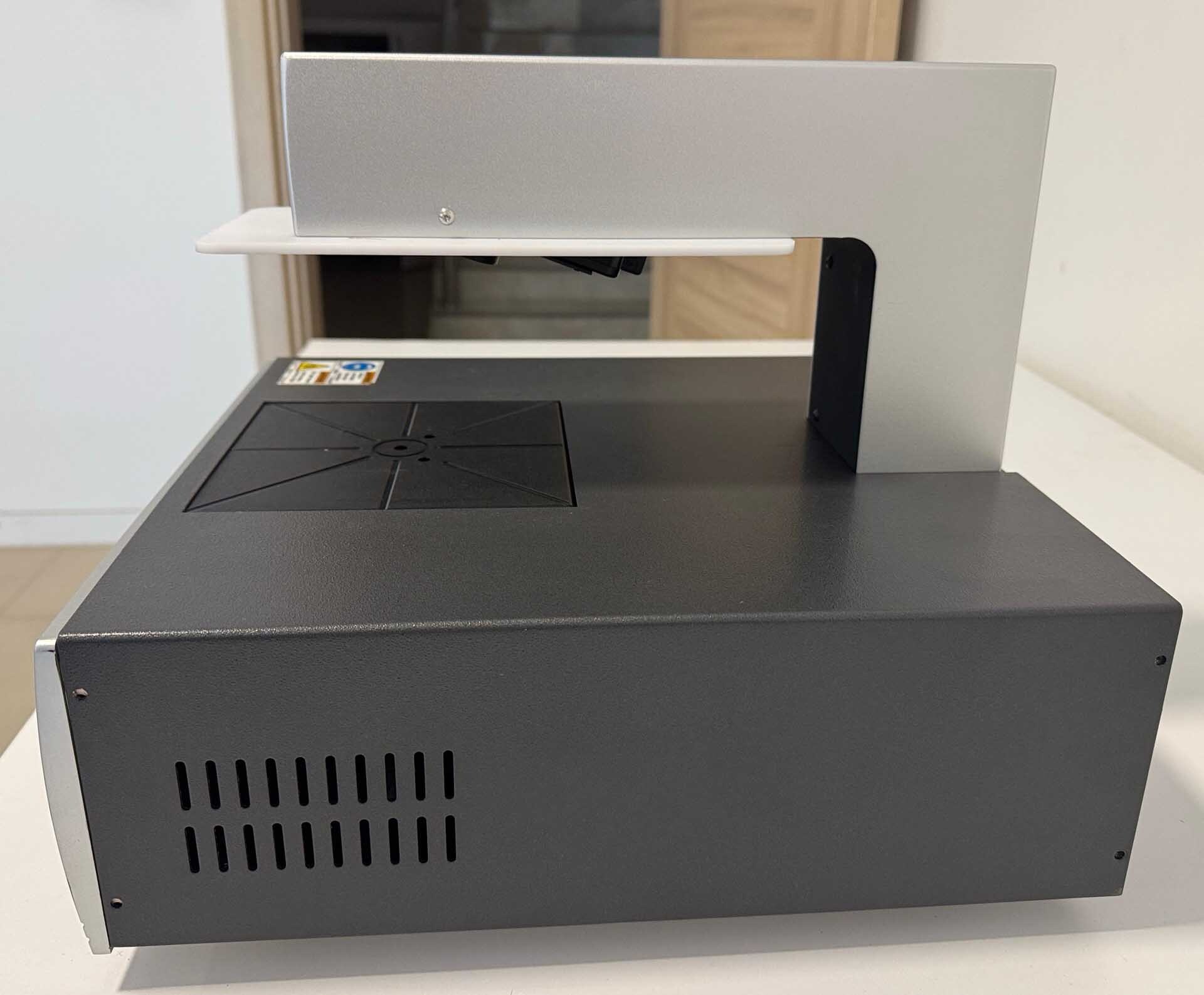
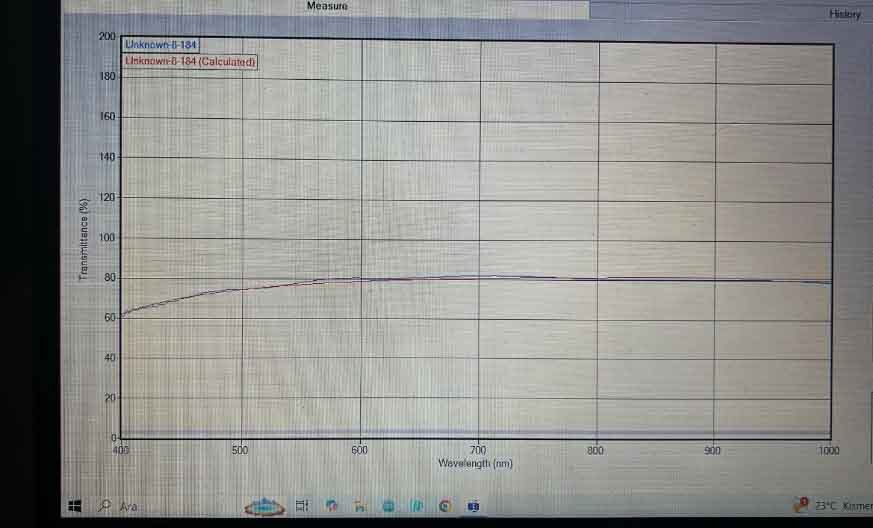
ID: 293768760
Thin film analyzer
Wavelength range: 190-1100 nm
Thickness measurement range: 1 nm-40 µm
Minimum thickness: 50 nm
Probe spot size: 6 mm
Interface: USB 1.0
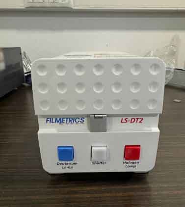
Light source
Accuracy:
Precision: 0.02 nm
Stability: 0.05 nm
Halogen light
Spectrometer:
Wavelength accuracy: 0.5 nm
Wavelength reproducibility: 0.1 nm
Wavelength resolution: 2.5 nm
Noise: <0.0002 A
Stray light: <0.25% at 500 nm
Amplitude resolution: 14 Bit
Does not include PC
Operating system: Windows XP, 64 Bit
CE Marked
Power supply: 100-240 VAC, 20 W, 50/60 Hz.
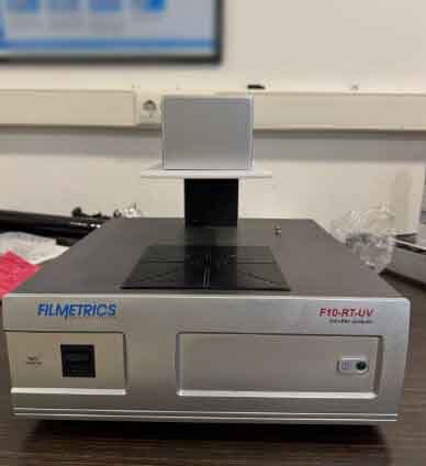
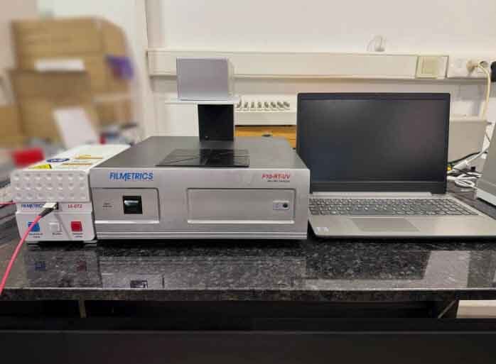
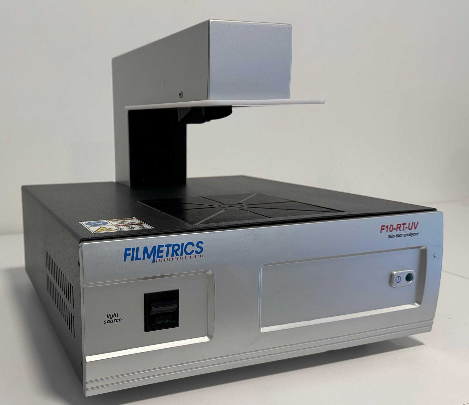
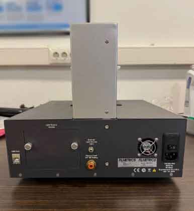
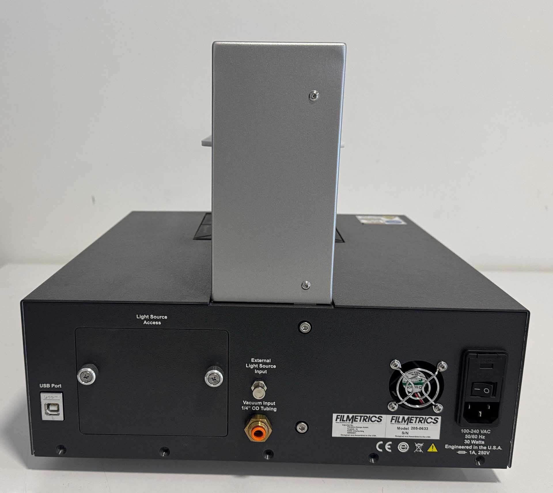
FILMETRICS F10-RT-UV is a cutting-edge wafer testing and metrology equipment designed to provide precise and accurate measurements for semiconductor manufacturing processes. This advanced system incorporates various innovative technologies and features that make it an essential tool for ensuring the quality and consistency of semiconductor wafers. One of the key features of F10-RT-UV is its ultraviolet (UV) measurement capability. UV spectroscopy is a powerful technique for characterizing thin films on semiconductor wafers, as it provides detailed information about film thickness, composition, and optical properties. FILMETRICS F10-RT-UV is equipped with a high-performance UV spectrometer that can accurately measure the UV absorption and reflectance of thin films with high sensitivity and resolution. In addition to UV spectroscopy, F10-RT-UV also incorporates real-time monitoring capabilities. This feature allows users to track the deposition and etching processes on the wafer in real-time, providing immediate feedback on process parameters and ensuring that the desired film properties are achieved. The real-time monitoring capability of FILMETRICS F10-RT-UV is essential for optimizing production processes and minimizing defects in semiconductor manufacturing. Another important aspect of F10-RT-UV is its wafer mapping functionality. This feature allows users to create detailed maps of film thickness and uniformity across the entire surface of the wafer. By analyzing these maps, users can identify variations and defects in the film deposition process, enabling them to make necessary adjustments to improve the overall quality of the wafers. FILMETRICS F10-RT-UV also offers automated data analysis and reporting capabilities. The unit can process large volumes of measurement data quickly and accurately, providing users with detailed reports and insights into the quality of the wafers. The automated data analysis feature of F10-RT-UV saves time and reduces the risk of human error, ensuring that users can make informed decisions based on reliable data. Furthermore, FILMETRICS F10-RT-UV is designed with user-friendly software and interface, making it easy for operators to configure measurements, analyze data, and generate reports. The intuitive software interface of the machine allows users to customize measurement parameters, set up measurement sequences, and view measurement results in an organized and user-friendly manner. Overall, F10-RT-UV is a state-of-the-art wafer testing and metrology tool that offers advanced UV spectroscopy capabilities, real-time monitoring, wafer mapping, automated data analysis, and user-friendly software interface. This powerful asset is essential for semiconductor manufacturers looking to improve the quality and consistency of their wafers and optimize their production processes.
There are no reviews yet