Used FRT CWL #293757446 for sale
URL successfully copied!
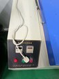
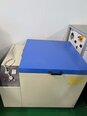
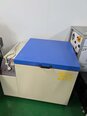
Tap to zoom
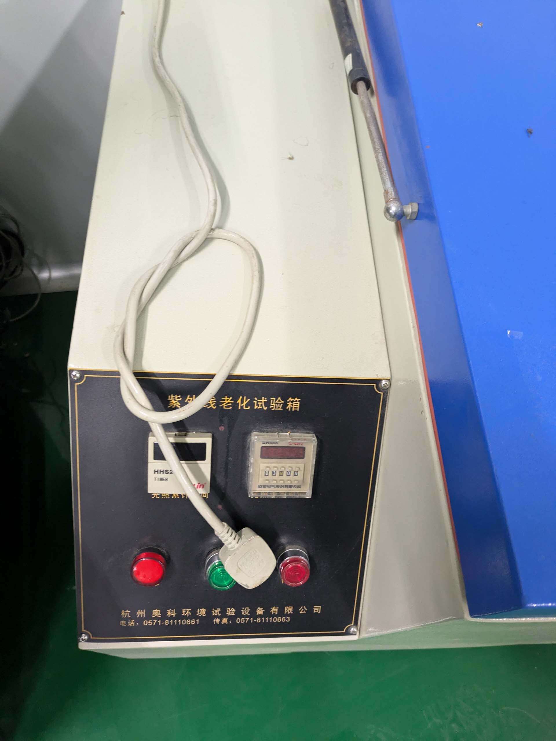

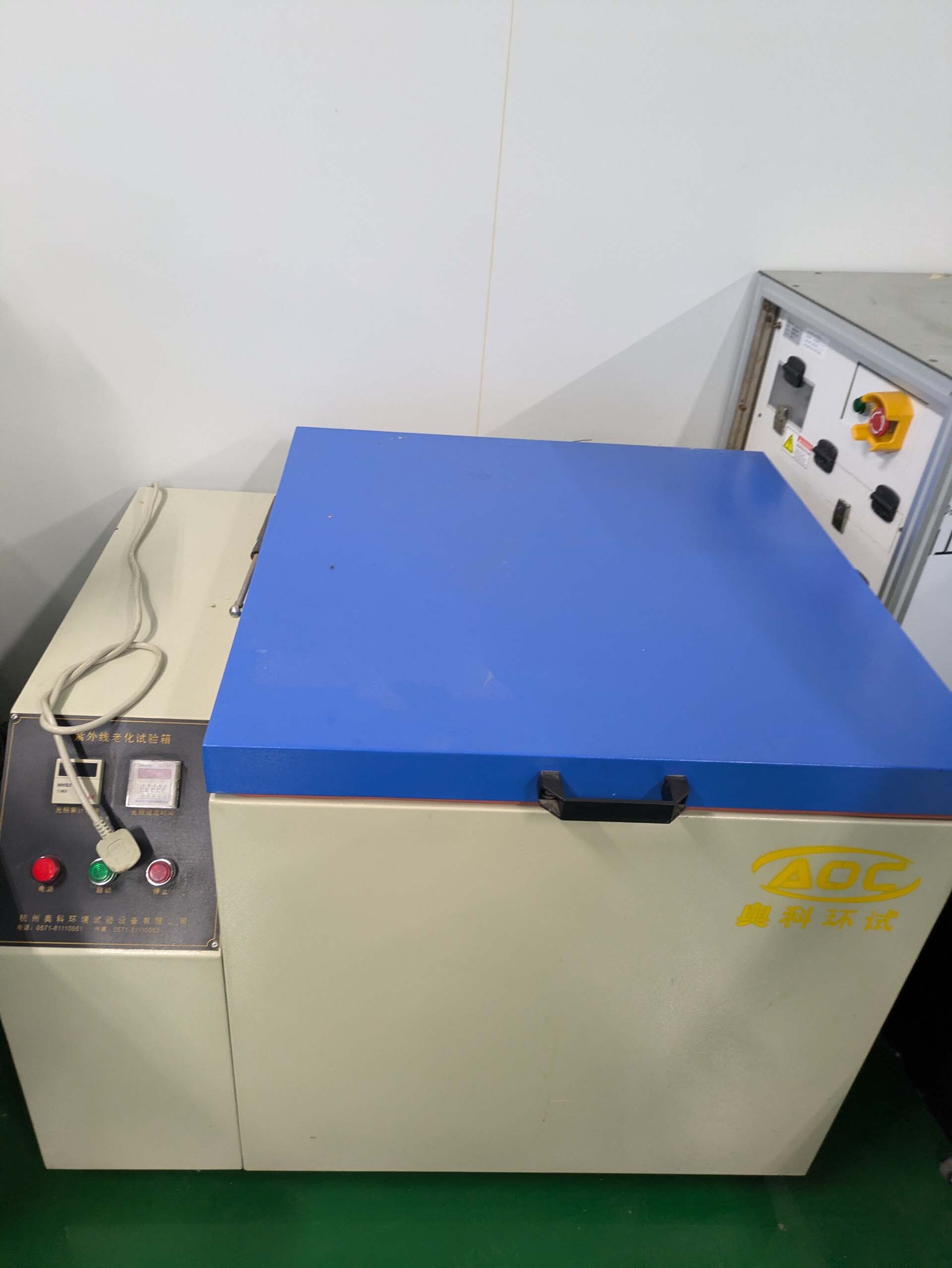
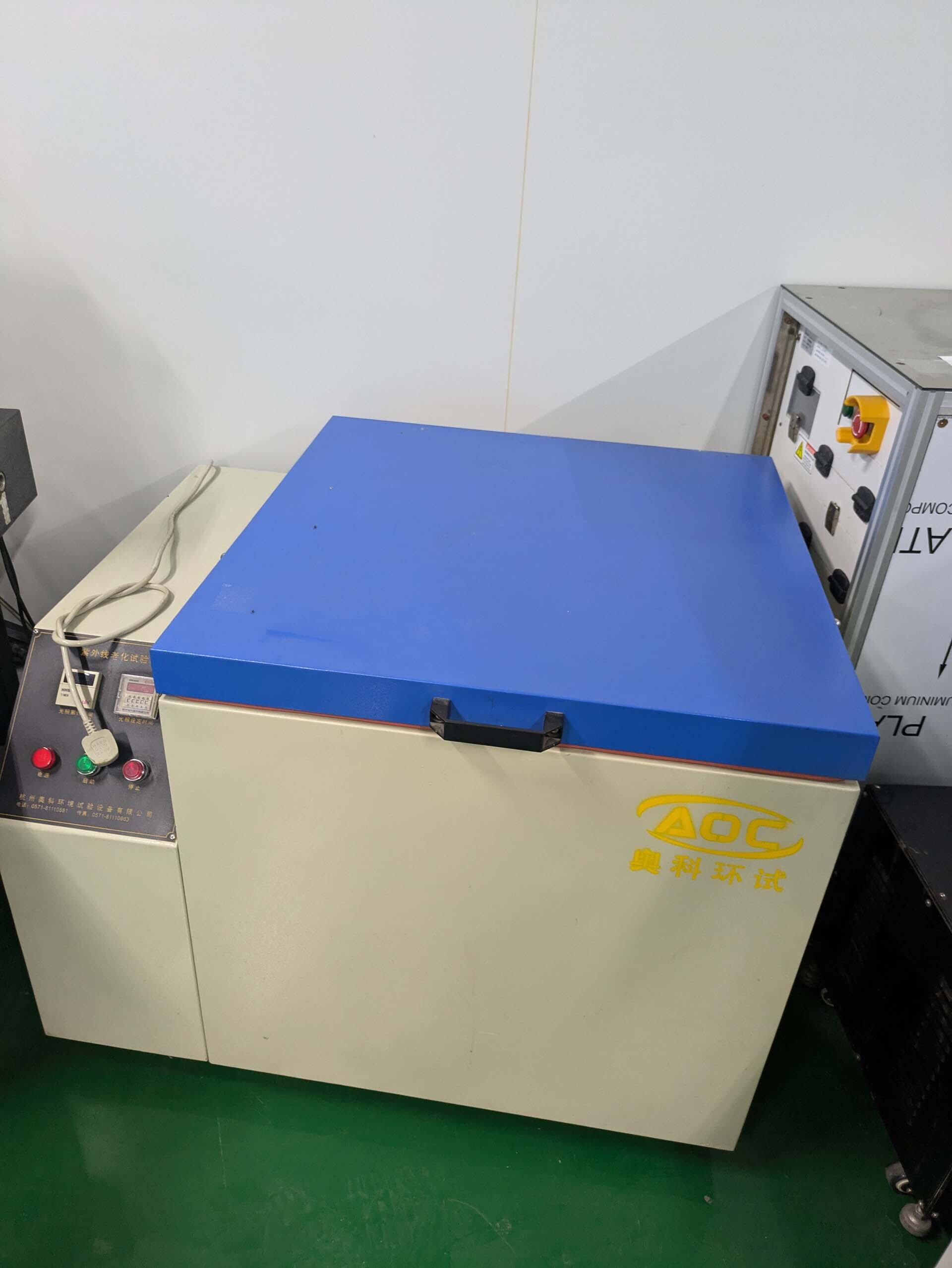
FRT CWL is a cutting-edge wafer testing and metrology equipment that plays a crucial role in the semiconductor industry by ensuring the quality and reliability of integrated circuits and other semiconductor devices. This advanced system is equipped with a range of powerful capabilities that enable engineers and technicians to conduct precise measurements and evaluations of wafer properties, ensuring that the end products meet strict performance and quality standards. CWL unit employs a combination of innovative technologies, including imaging, spectroscopy, and profilometry, to provide comprehensive insight into the characteristics of semiconductor wafers. Using a non-destructive approach, this machine analyzes various parameters such as surface roughness, film thickness, defect density, and topography, offering valuable data that is essential for process optimization and quality control. One of the key features of FRT CWL tool is its high-resolution imaging capabilities, which allow users to visualize and analyze the surface morphology of wafers with exceptional detail. By capturing images at different magnifications and angles, the asset provides insights into the structural characteristics of the wafer, such as patterns, features, and defects, enabling engineers to identify potential issues and make informed decisions about process adjustments. In addition to imaging, CWL model incorporates spectroscopic techniques to analyze the chemical composition of wafer surfaces. By measuring the reflectance, absorption, or emission of light at different wavelengths, the equipment can identify the presence of various materials and contaminants on the wafer, offering insights into the composition and purity of the semiconductor layers. Furthermore, the profilometry capabilities of FRT CWL system enable engineers to measure the thickness, roughness, and step height of thin films and patterns on the wafer surface. By utilizing advanced scanning techniques and algorithms, the unit generates highly accurate 3D topographic maps of the wafer, allowing users to evaluate the uniformity and quality of deposited layers with precision. CWL machine is designed to be user-friendly, with intuitive software interfaces that enable easy operation and data analysis. The tool offers customizable measurement protocols and data visualization tools, allowing users to tailor the analysis to meet specific requirements and extract relevant insights from the measured data. In conclusion, FRT CWL is a state-of-the-art wafer testing and metrology asset that provides semiconductor manufacturers with the tools needed to ensure product quality, performance, and reliability. By combining advanced imaging, spectroscopic, and profilometry capabilities, this model enables engineers to conduct comprehensive evaluations of wafer properties, supporting process optimization, defect analysis, and quality assurance in the semiconductor manufacturing industry.
There are no reviews yet