Used FRT MicroProf 300 #293821952 for sale
URL successfully copied!
Tap to zoom
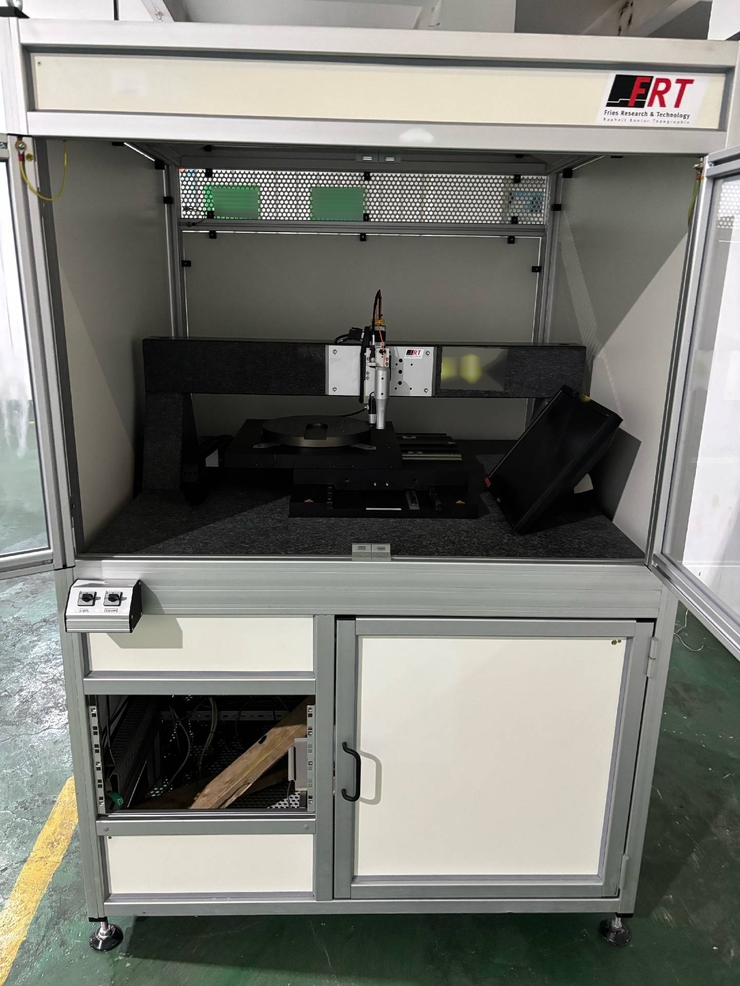

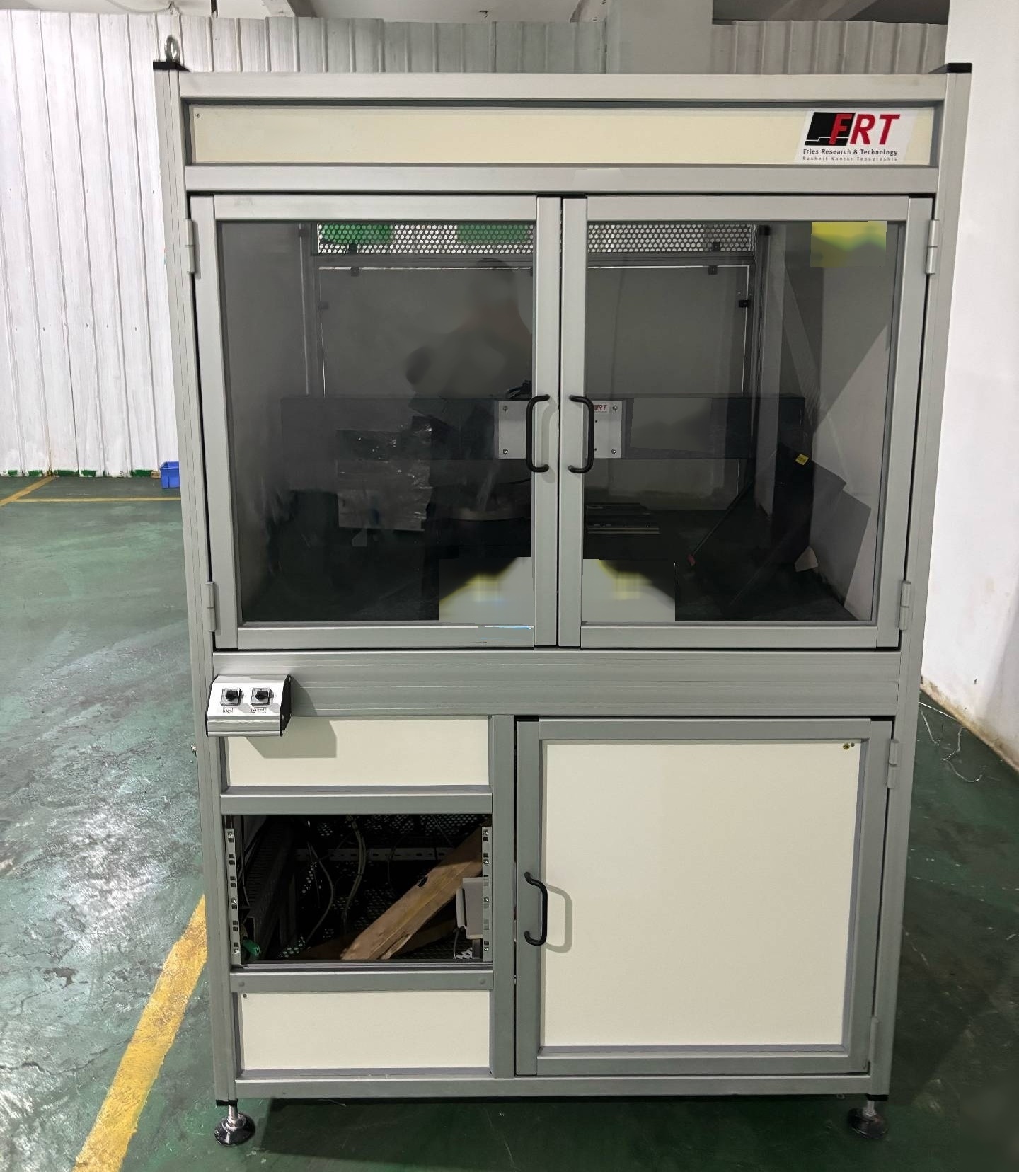
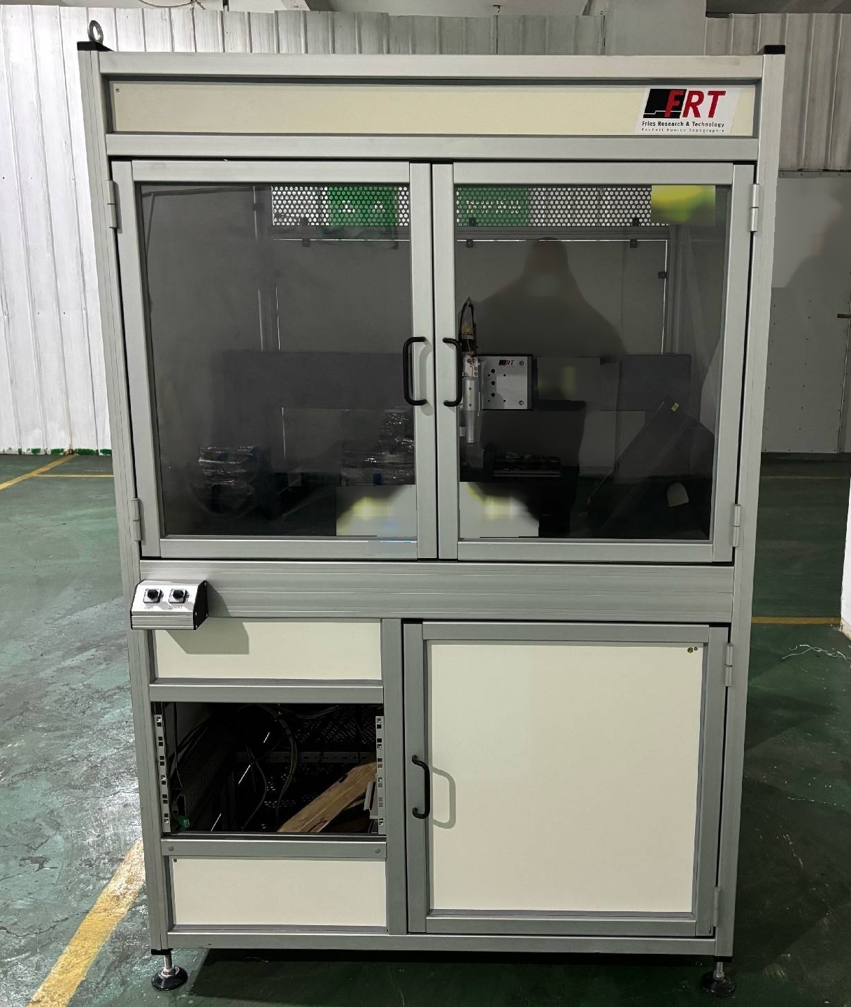
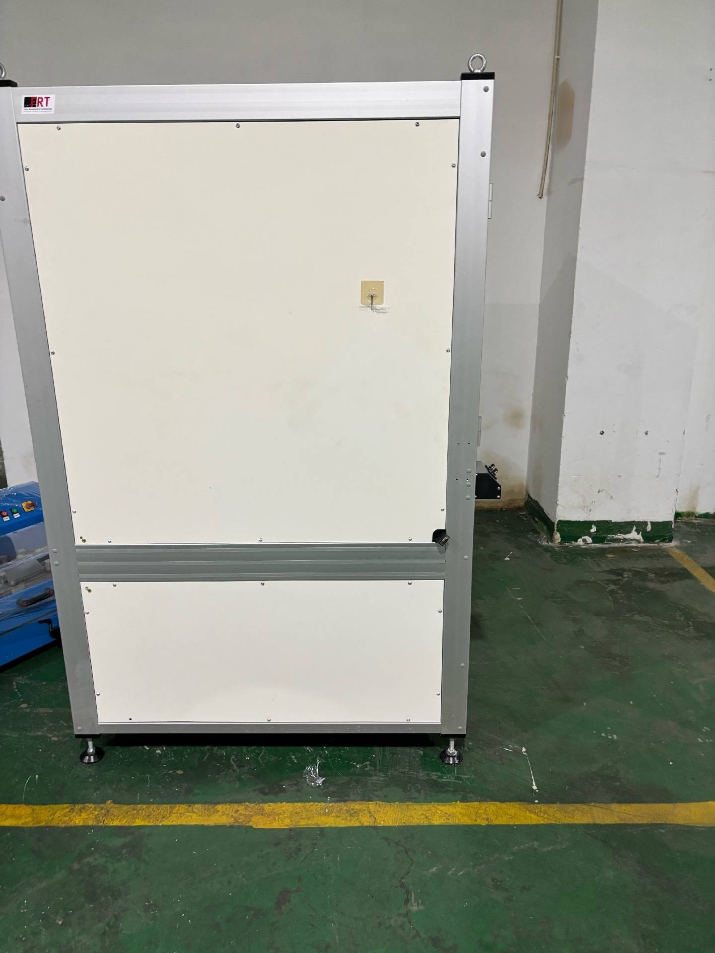
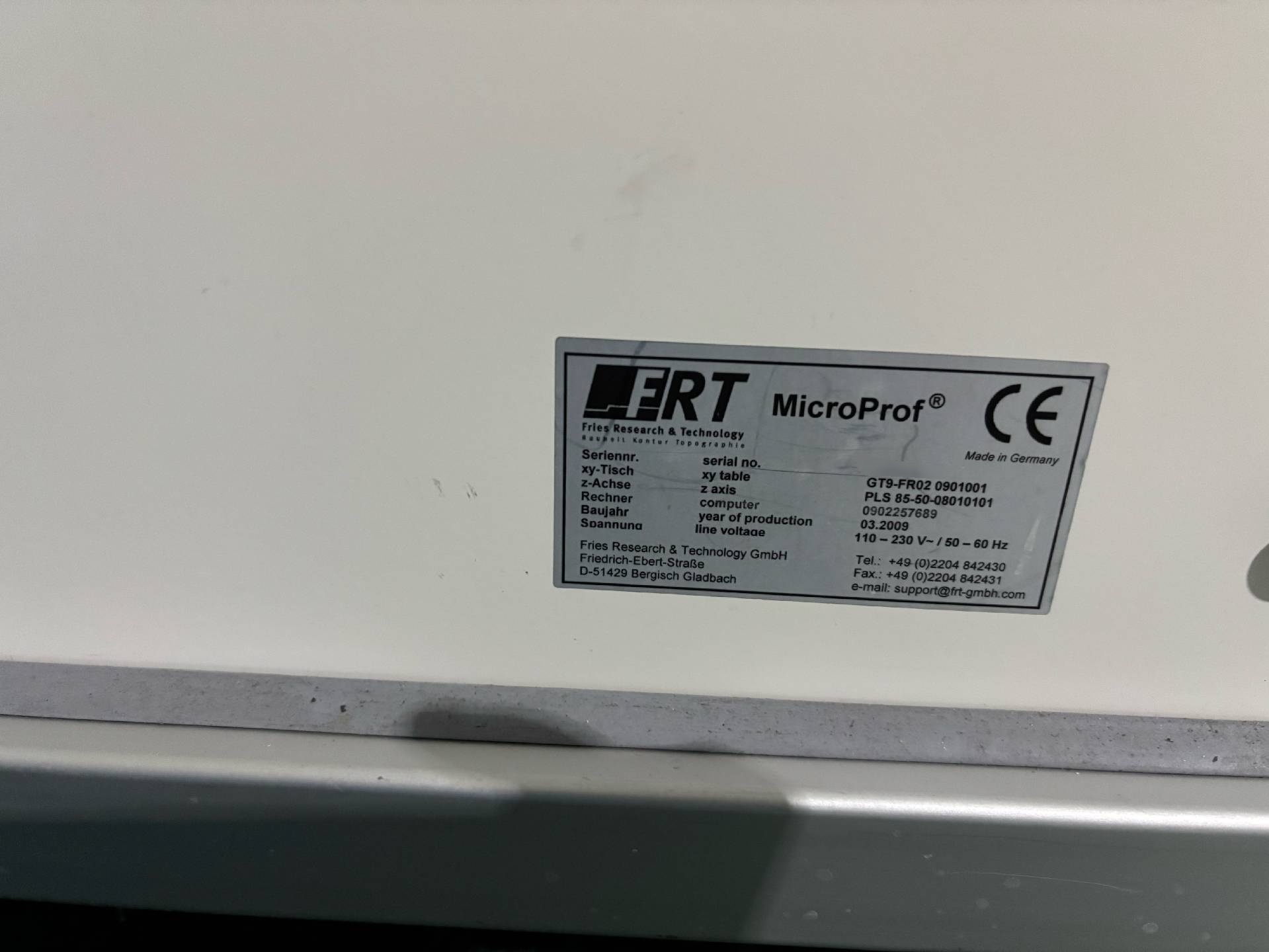
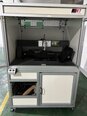
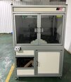
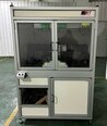
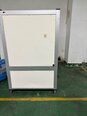
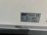
FRT MicroProf 300 is a cutting-edge wafer testing and metrology equipment designed to provide precise and accurate measurement and analysis of surface topography, roughness, film thickness, and other critical parameters on semiconductor wafers. This powerful tool is specifically engineered to meet the demanding requirements of the semiconductor industry and is capable of delivering high-performance results for both research and production environments. MicroProf 300 utilizes advanced imaging and measurement technologies to enable comprehensive analysis of wafer surfaces with exceptional precision. Equipped with a range of sensors, detectors, and scanning probes, this system is able to capture detailed 3D topographical data with sub-nanometer resolution. The ability to generate high-resolution maps of surface features, defects, and patterns allows for in-depth characterization of wafer quality and performance, aiding in process development, quality control, and yield optimization. One of the key capabilities of FRT MicroProf 300 is its ability to perform fast and accurate thickness measurements of thin films deposited on semiconductor wafers. Using non-contact optical techniques, the unit can determine film thickness with high repeatability and reproducibility, making it an essential tool for process monitoring and evaluation. By analyzing the uniformity and thickness variation of thin films across the wafer surface, users can identify and address issues related to film deposition, adhesion, and quality. In addition to film thickness measurement, MicroProf 300 offers comprehensive roughness analysis capabilities for characterizing the surface texture of wafers at the micro and nano scales. By analyzing parameters such as roughness average (Ra), root mean square (RMS) roughness, and peak-to-valley height, the machine can provide valuable insights into surface quality, flatness, and roughness distribution. This information is vital for ensuring the reliability and performance of semiconductor devices manufactured on these wafers. Another critical feature of FRT MicroProf 300 is its ability to perform automated defect inspection and metrology on semiconductor wafers. By combining advanced imaging algorithms with high-speed scanning capabilities, the tool can detect and categorize defects such as particles, scratches, pits, and pattern anomalies on the wafer surface. This allows users to identify and quantify defects that may impact device yield and reliability, facilitating targeted process improvements and defect mitigation strategies. Furthermore, MicroProf 300 is equipped with a user-friendly software interface that enables intuitive control, visualization, and analysis of measurement data. The asset supports customizable measurement recipes, automated data processing, and interactive data visualization tools to streamline the workflow and facilitate data interpretation. Users can generate comprehensive reports, statistical analyses, and graphical representations of measurement results to support decision-making and process optimization. In summary, FRT MicroProf 300 is a state-of-the-art wafer testing and metrology model that offers advanced capabilities for analyzing surface topography, roughness, film thickness, and defects on semiconductor wafers. With its high precision, versatility, and reliability, this equipment is an indispensable tool for semiconductor manufacturers, research institutions, and quality control laboratories seeking to achieve the highest standards of wafer quality, process control, and device performance.
There are no reviews yet