Used FRT MicroSpy Topo DT #293762916 for sale
URL successfully copied!
Tap to zoom
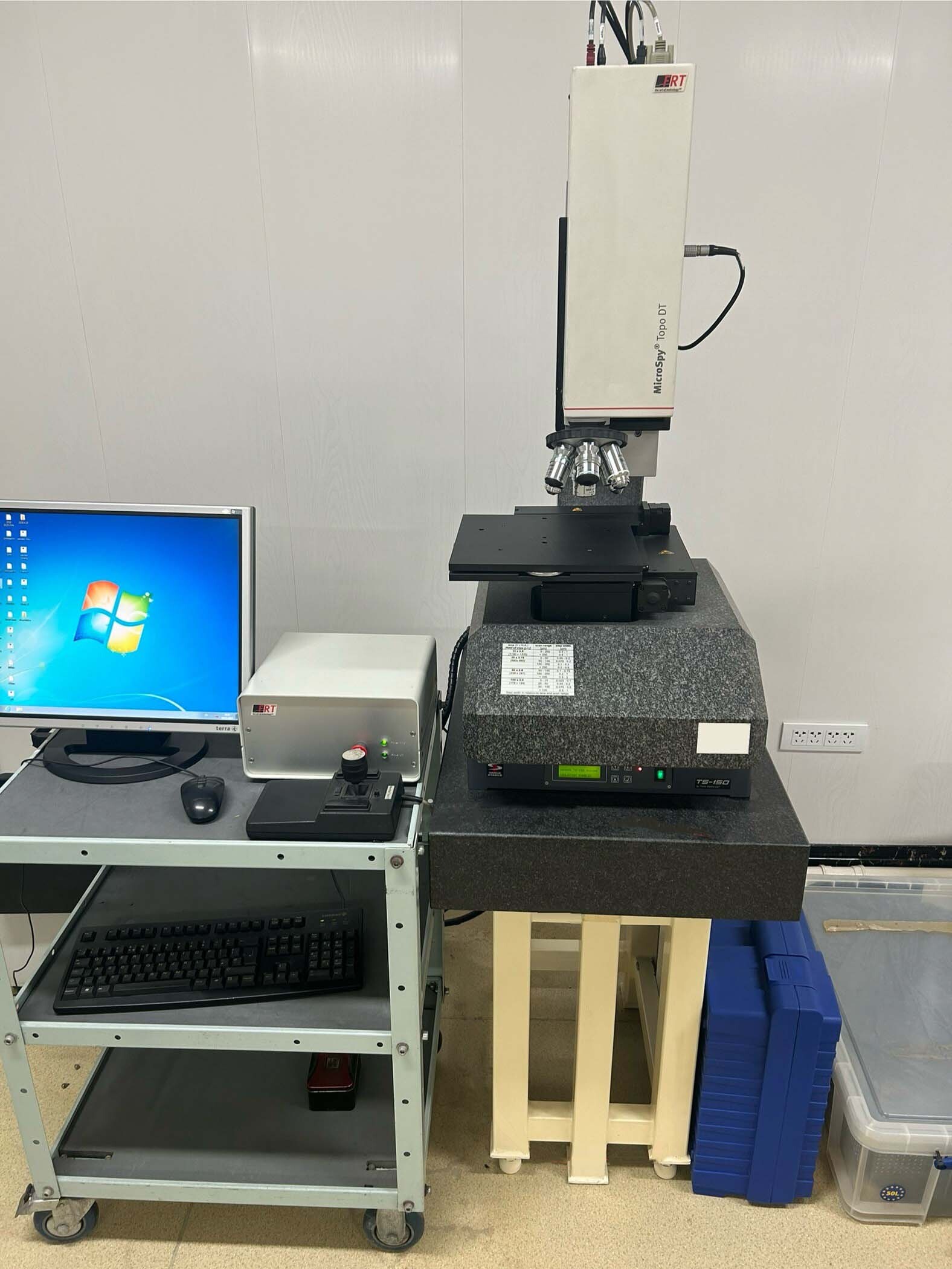

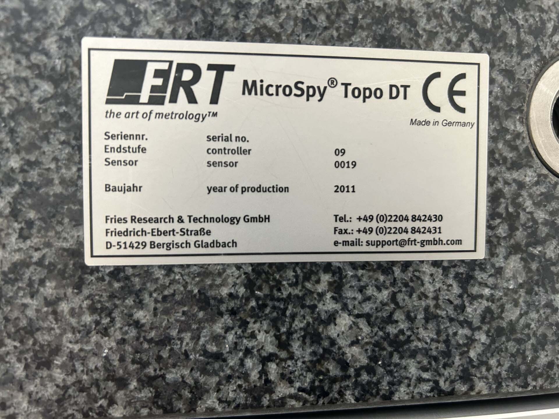
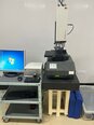
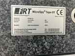
FRT MicroSpy Topo DT is an advanced wafer testing and metrology equipment designed to provide high-precision topographical measurements of semiconductor wafers. This cutting-edge system integrates innovative technology to offer semiconductor manufacturers a comprehensive solution for characterizing wafer surfaces with unparalleled accuracy and efficiency. At the core of MicroSpy Topo DT unit is a sophisticated optical profiler that utilizes advanced imaging techniques to capture detailed topographical information from the surface of the wafer. The machine employs a combination of white light interferometry and confocal microscopy to achieve sub-nanometer resolution, allowing it to detect even the smallest surface features and defects on the wafer. One of the key features of FRT MicroSpy Topo DT is its ability to perform fully automated wafer mapping and analysis. The tool is equipped with a robotic stage that can precisely position the wafer under the microscope, allowing for rapid and repeatable measurements across the entire surface of the wafer. This automated mapping capability enables semiconductor manufacturers to efficiently inspect large numbers of wafers and quickly identify any deviations from the desired surface profile. MicroSpy Topo DT asset also offers a wide range of measurement modes and analysis tools to support various wafer testing and metrology applications. Users can choose from a selection of measurement techniques, such as 3D surface profiling, step height analysis, roughness measurement, and defect inspection, to suit their specific requirements. The model's intuitive software interface allows users to customize measurement parameters, visualize measurement results in real-time, and generate detailed reports for further analysis. In addition to its advanced imaging capabilities, FRT MicroSpy Topo DT equipment is equipped with powerful image processing algorithms that enable automatic data analysis and defect recognition. The system can detect and classify various types of surface defects, including scratches, particles, pits, and pattern deviations, with high accuracy and consistency. This automated defect detection functionality helps semiconductor manufacturers to improve yield rates, enhance process control, and ensure the quality of their wafers. Moreover, MicroSpy Topo DT unit is designed to be highly flexible and adaptable to different wafer sizes, materials, and surface finishes. The machine's modular design allows users to easily configure and customize the tool to meet their specific testing requirements, making it suitable for a wide range of wafer testing and metrology applications in the semiconductor industry. Overall, FRT MicroSpy Topo DT asset represents a state-of-the-art solution for wafer testing and metrology, offering semiconductor manufacturers a comprehensive tool for characterizing wafer surfaces with exceptional precision, speed, and reliability. With its advanced imaging technology, automated mapping capabilities, versatile measurement modes, and automated defect detection features, MicroSpy Topo DT model enables semiconductor manufacturers to achieve higher productivity, improve process control, and deliver superior quality wafers for advanced semiconductor devices.
There are no reviews yet