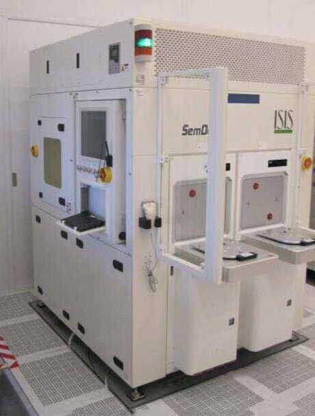
Used ISIS SENTRONICS SemDex A32-34 #9407579 for sale
It looks like this item has already been sold. Check similar products below or contact us and our experienced team will find it for you.
Tap to zoom


Sold
ID: 9407579
Wafer Size: 8"-12"
Vintage: 2011
Wafer testing and metrology system, 8"-12"
Automatic loading
(2) Load ports (12" FOUB and 8" Open cassette via 12" Mechanical adaptor)
Measurement part:
Automated measurement:
Substrate / Layer / Total thickness
Bow / Warp
Mini-bumps / Vias (Micro 3D metrology) and nm roughness
Integrated sensor heads:
Layer thickness / Bow: StraDex f2 - 80 (Top), StraDex f24 - 300 (Bottom)
3D micro-topography: StraDex a3 (Top, off-center by about 90 mm)
Camera function (Top sensor)
Autofocus:
StraDex a3 (Precision mechanical bearing)
StraDex f2 - 80
StraDex f24 - 300 (Air bearing)
Anti-vibration plate below chuck
Optical wavelengths:
Top sensor: 830 nm (Minimum Silicon thickness 2.5 μm)
Bottom sensor: 1300 nm (Minimum Silicon thickness 7 μm)
Top sensor (Off-center): ~ 500 nm
Integrated calibration samples:
Thickness sample silicon: 123 μm (Roughness in the several nm level)
Thickness sample silicon: 750 μm (Roughness in the several nm level)
Step profiles for 3D Micro topography
Cross hair for top and bottom thickness sensor alignment
Sensor system with (3) StraDex sensor heads (Triple sensor setup):
StraDex f2 - 80 (Top):
Spot size: 8 μm
Autofocus range: 2 - 22 mm
Maximum warp: 3 mm
Acquisition rate: < 4 kHz
Thickness (Undoped silicon):
Fast mode: 2.5 - 80 μm
Slow mode: 2.5 - 80 μm
Thickness (Glass, polymer):
Fast mode: 5 - 200 μm
Slow mode: 5 - 200 μm
StraDex f24 - 300 (Bottom):
Spot size: 24 μm
Autofocus range: 24 - 44 mm
Maximum warp: 2 mm
Acquisition rate: < 4 kHz
Thickness (Silicon):
Fast mode: 8 - 350 μm
Slow mode: 8 - 800 μm
Thickness (Glass, polymer):
Fast mode: 14 - 300 μm
Slow mode: 14 - 1000 μm
StraDex a3 (Top):
Field-of-view: (0.35 mm)²
Lateral pixel size: 0.3 μm
Working distance: 3.5 mm
Autofocus range: 4 mm
Maximum Z-height: 60 μm (High-res.) / 120 μm (Low-res.)
Repeatability: 0.5 nm (High-res.)
Total acquisition time: 2 - 3 sec.
Maximum focusing speed: 200 μm/s
Surface roughness: Rz < 0.1 μm
Confidence range: 2 Sigma
Single sensor mode:
Absolute accuracy: < ± 0.5 μm
Repeatability (Fast mode): < ± 0.1 μm
Repeatability (Slow mode): < ± 0.5 μm
Twin sensor (Layer thickness) mode:
Absolute accuracy: < ± 1 μm
Repeatability (Fast and slow mode): < ± 0.5 μm
Stage:
Maximum X/Y travel range: 300 x 300 mm²
Maximum velocity: 30 mm/s
Lateral accuracy: 4 μm
Maximum height variation repeatable: 2 μm
Free positioning via keypads
Anti-vibration table
Air suspension
Perforated vacuum chuck for double side measurements of 6", 8" and 12" unframed and framed wafers
10 mm Holes at 20 mm inter-center spacing
Vacuum for wafer suction
3 Lift pins to elevate the wafer (≥ 200 mm in diameter) by 9.5 mm
Wafer handling:
Up to 60 wafers / hour
Single ATM robot with vacuum gripper
Pre-aligner
OCR reader (Standard: Top scribe readout)
General:
Industrial computer (2 GHz) with screen
Data interface: LAN
Fan filter unit, ISO class 10
Temperature: 10°C - 35°C
Power supply voltage: 100 V - 240 V, 50-60 Hz
Maximum power consumption: 5 kW
Sensor missing
2011 vintage.
ISIS SENTRONICS SemDex A32-34 is a wafer testing and metrology equipment designed for component analysis, surface metrology, and electrical evaluation. It is capable of testing and measuring various wafer substrates including thin and thick-film, monolithic and embedded-circuit, and polysilicon. SemDex A32-34 incorporates a fully automated testing and metrology system, allowing for precise and repeatable results. It uses an X-Y-Z scanning stage for precise wafer positioning and movement, providing accurate alignment and repeatability between wafer locations. This stage is controllable by a PC based controller (PCBC) and is capable of scanning up to 100 individual areas of the wafer. ISIS SENTRONICS SemDex A32-34 includes a high performance elecro-optical detection package, including a high-resolution CMOS camera and bright-field microscope, giving it the capability to detect and analyze large areas of a single wafer. This package also includes a voltage mode characterization unit, allowing for precise measurement of wafer parameters. The machine is also equipped with an advanced algorithm-based software package, providing users with the capability to analyze their scan data in a variety of ways including surface metrology calculations, fault detection, and statistical process control. In addition, the tool provides real-time visualization of the scan data, allowing the user to quickly review the results. Other key features of SemDex A32-34 include its ability to provide a wide array of test and measurement capabilities, such as 4-point probe measurement and electrical current mapping, as well as cutting-edge imaging algorithms for the detection of ultra-small defects and contaminants. In conclusion, ISIS SENTRONICS SemDex A32-34 is a comprehensive wafer testing and metrology asset designed for precise and repeatable results. It incorporates a number of advanced features for testing various wafer substrates, such as a fully automated X-Y-Z scanning stage, high resolution imaging model and an algorithm-based software package, allowing users to analyze their scan data quickly and accurately.
There are no reviews yet