Used KEYENCE CL-P030N #293824334 for sale
URL successfully copied!
Tap to zoom
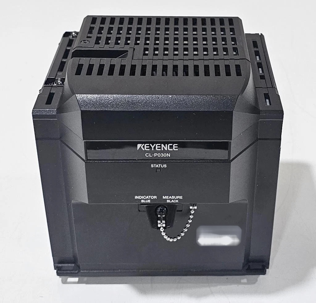

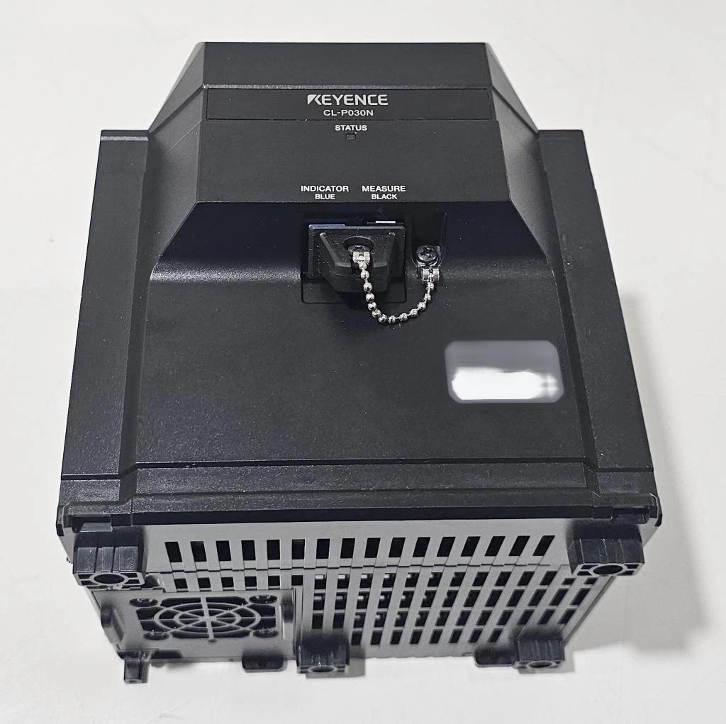
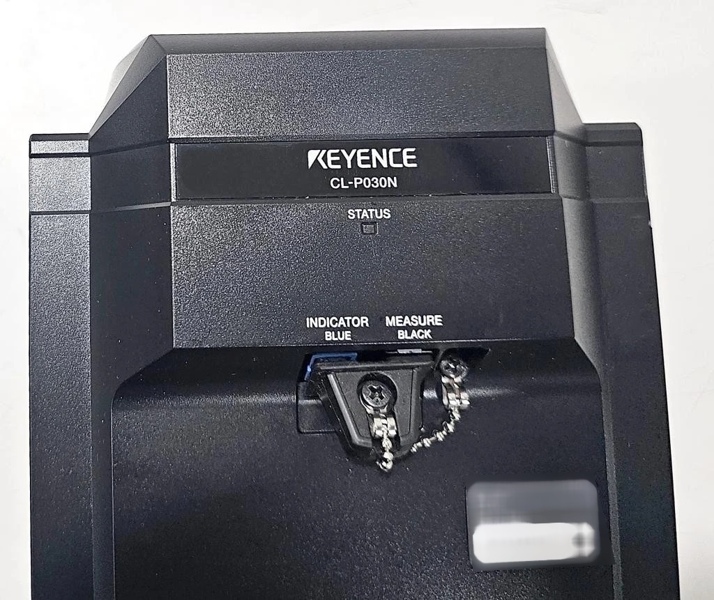
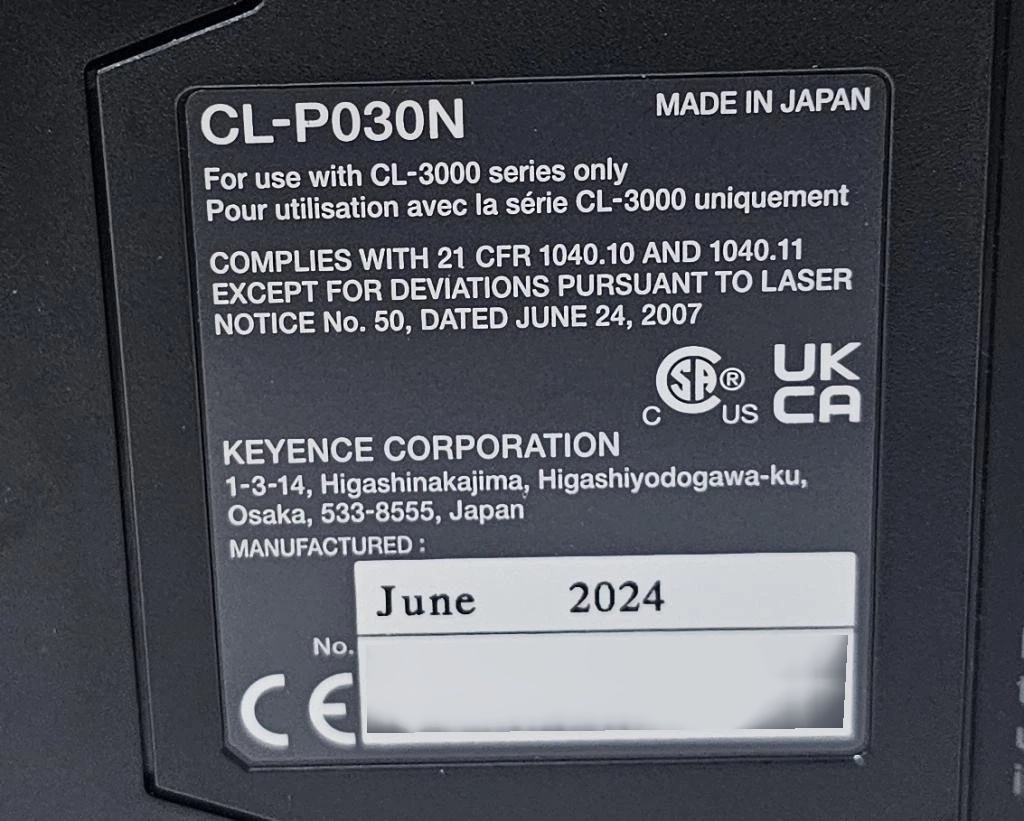
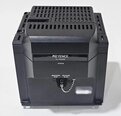
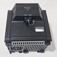
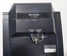
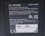
KEYENCE CL-P030N is a cutting-edge wafer testing and metrology equipment designed to meet the stringent requirements of the semiconductor industry. This advanced system incorporates state-of-the-art technology to deliver precise and reliable measurements for evaluating the quality and characteristics of semiconductor wafers. At the heart of CL-P030N unit is a high-resolution imaging machine that allows for detailed inspection and analysis of wafers. The tool is equipped with a powerful optical asset that can capture images with exceptional clarity and accuracy, enabling precise measurement of critical dimensions and features on the wafer surface. One of the key features of KEYENCE CL-P030N model is its ability to perform automated measurements, reducing the time and effort required for wafer inspection. The equipment is capable of scanning wafers quickly and efficiently, generating comprehensive data reports that can be used for process optimization and quality control. CL-P030N system is also equipped with advanced image processing algorithms that enhance the accuracy and reliability of measurements. These algorithms are designed to compensate for factors such as distortion and noise, ensuring that the unit delivers consistent and precise results regardless of environmental conditions. In addition to its imaging and measurement capabilities, KEYENCE CL-P030N machine offers a range of advanced functionalities for wafer testing and metrology. The tool is equipped with sophisticated software that allows users to customize measurement parameters, visualize data in multiple formats, and generate detailed reports for analysis and documentation. Furthermore, CL-P030N asset is designed for ease of use, with a user-friendly interface that makes it easy for operators to set up measurements, analyze data, and generate reports. The model also features intuitive controls and workflows that streamline the testing process, reducing the risk of errors and improving overall efficiency. KEYENCE CL-P030N equipment is highly versatile, capable of performing a wide range of measurements and inspections on different types of wafers. Whether evaluating critical dimensions, surface roughness, or defect detection, the system can meet the diverse needs of semiconductor manufacturers and researchers. Overall, CL-P030N wafer testing and metrology unit represents a significant advancement in semiconductor testing technology. With its advanced imaging capabilities, automated measurements, and user-friendly interface, the machine offers a comprehensive solution for enhancing the quality and productivity of wafer manufacturing processes.
There are no reviews yet