Used KEYENCE LJ-S015 #293822578 for sale
URL successfully copied!
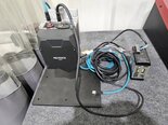
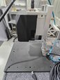
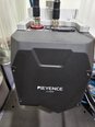
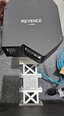
Tap to zoom

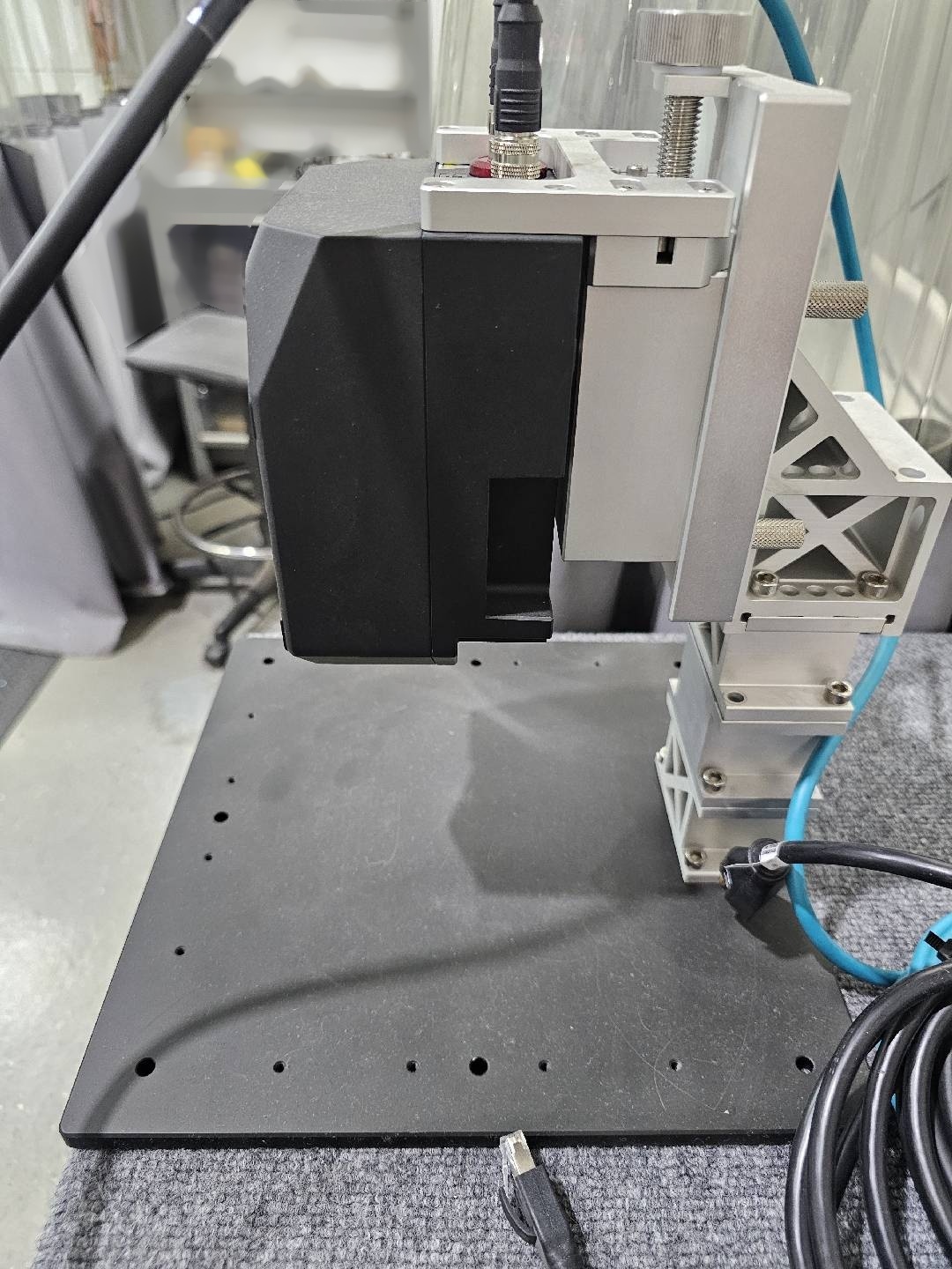
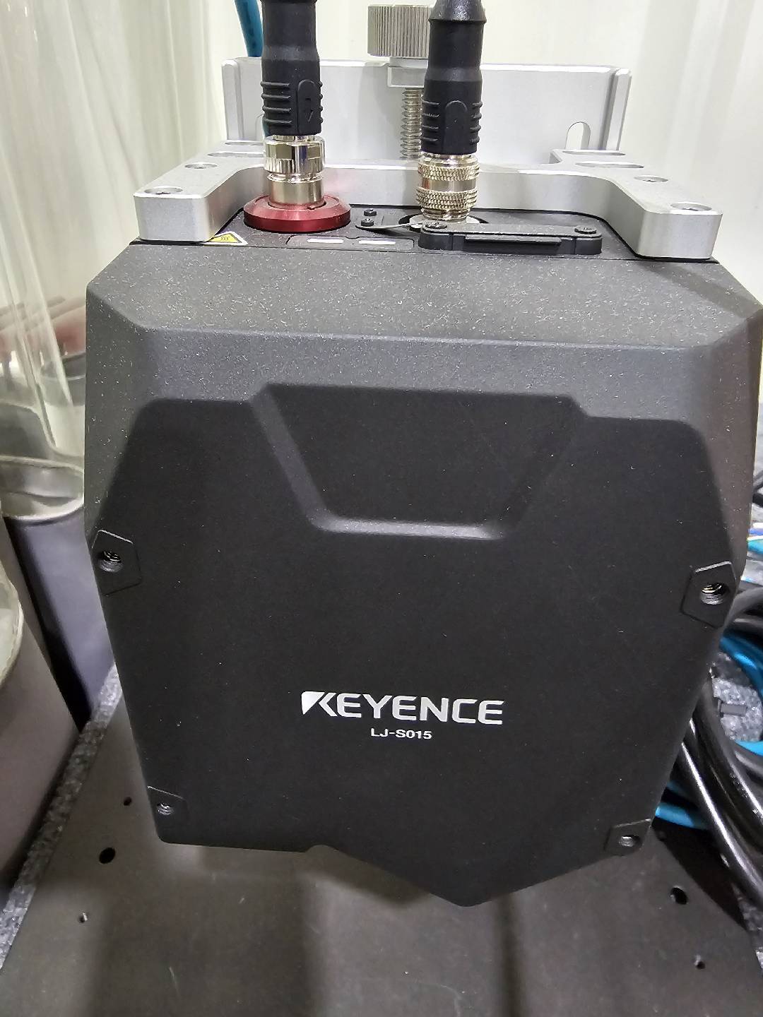
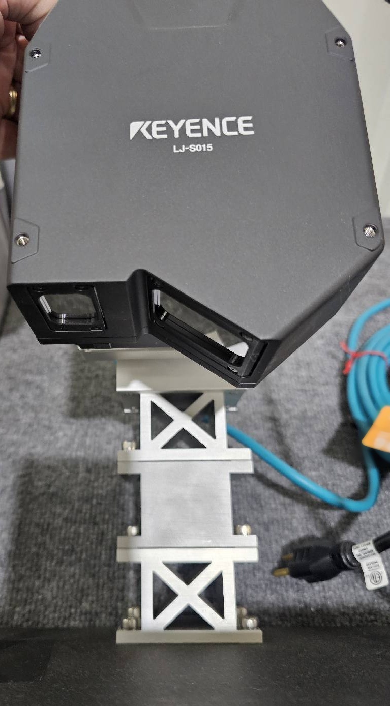
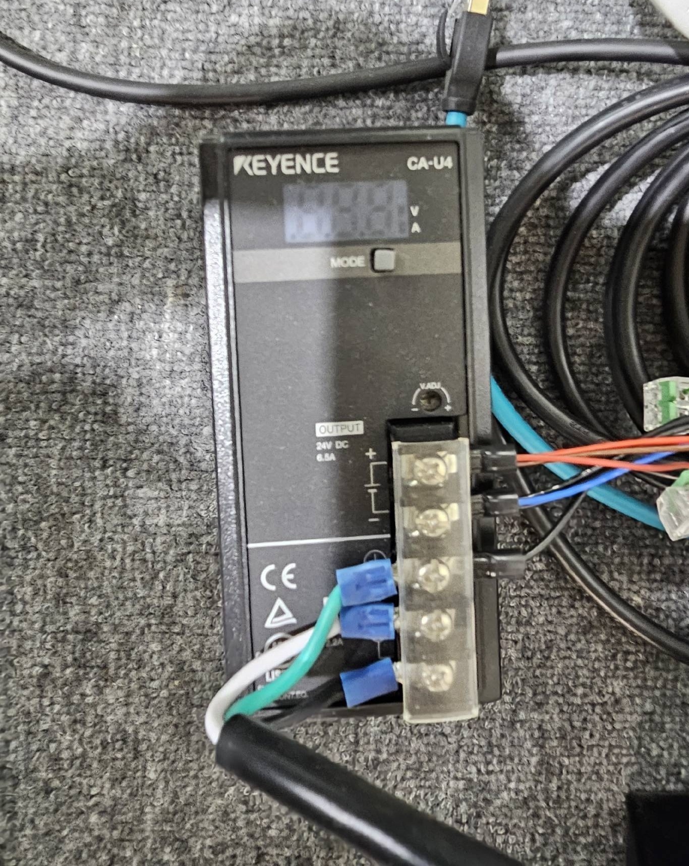
ID: 293822578
Vintage: 2024
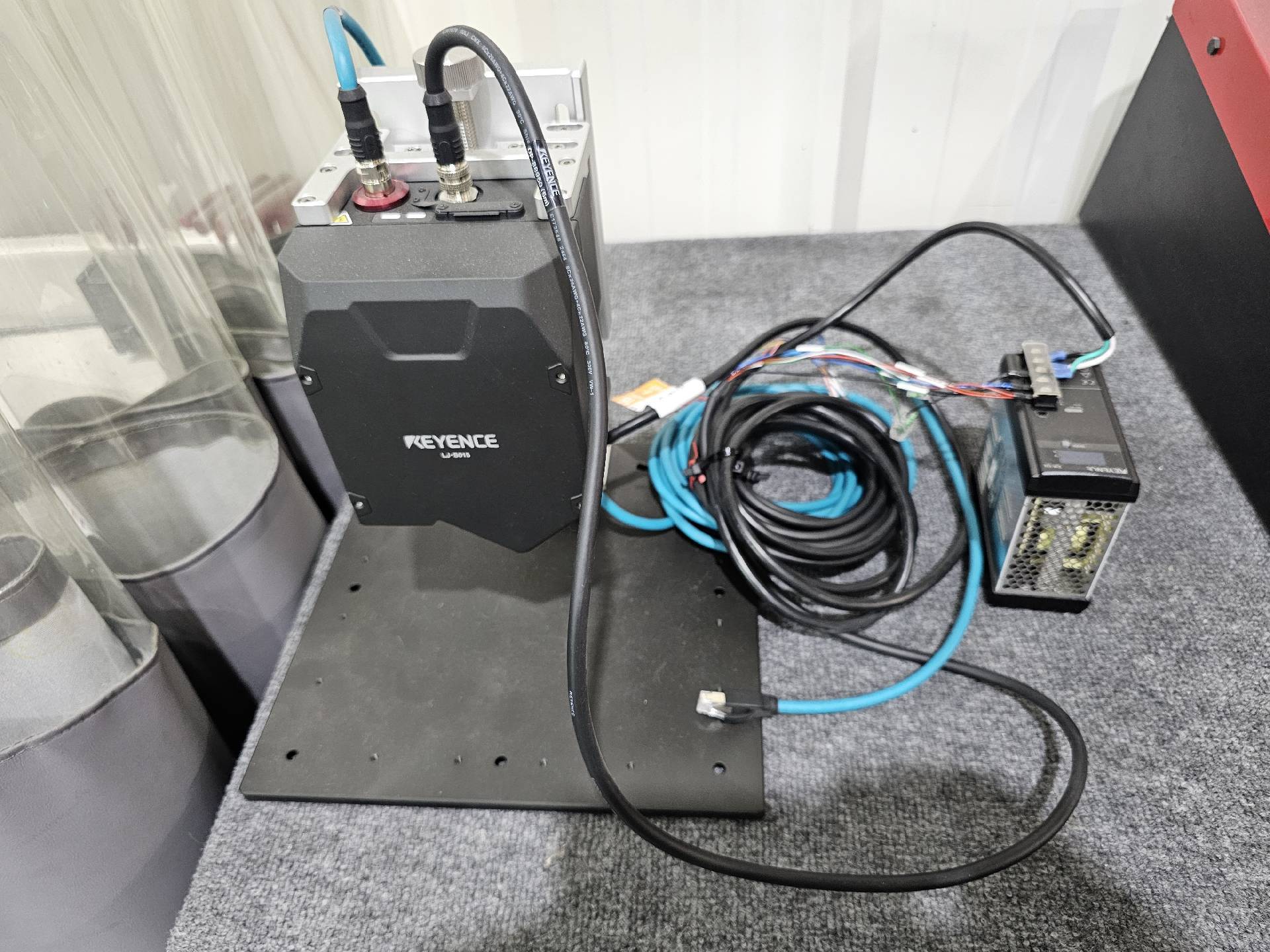
Sensor head
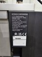
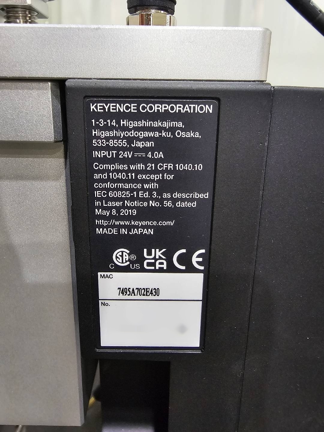
LJ-S015 3D laser snapshot sensor
OP-88836 Ethernet cable
OP-88950 Power supply cable
OP-88960 Dedicated stand mounting plate A
OP-88956 Adjuster
OP-88957 Base plate
OP-88958 Block
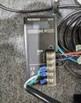
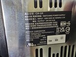
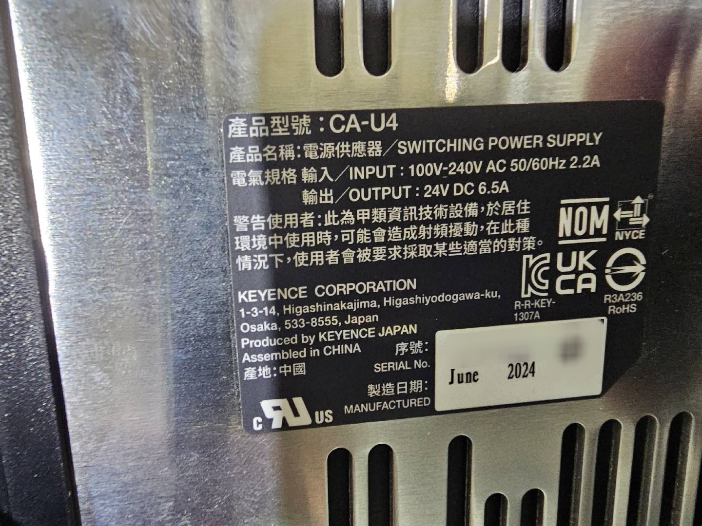
CA-U4# Switching Power Supply, 24V
2024 vintage.
KEYENCE LJ-S015 is a state-of-the-art wafer testing and metrology equipment designed to meet the demands of the semiconductor industry. This advanced system offers high-precision measurement capabilities for the characterization and quality control of wafers used in the production of semiconductors. With its cutting-edge technology and innovative features, LJ-S015 is engineered to provide accurate and reliable measurements essential for ensuring the performance and reliability of semiconductor devices. At the core of KEYENCE LJ-S015 unit is its sophisticated optical metrology technology, which enables non-contact measurement of critical parameters such as thickness, flatness, and surface roughness of semiconductor wafers. The machine is equipped with high-resolution cameras, laser sensors, and advanced image processing algorithms that allow for precise and rapid measurement of various wafer properties with sub-micron resolution. This comprehensive metrology capability makes LJ-S015 an indispensable tool for wafer inspection and quality assurance in semiconductor manufacturing processes. One of the key features of KEYENCE LJ-S015 tool is its automated measurement capability, which streamlines the testing process and reduces the need for manual intervention. The asset is equipped with advanced robotics and motion control systems that enable precise positioning of wafers for measurement, ensuring consistent and repeatable results. Additionally, LJ-S015 model supports wafer mapping and defect detection functionalities, allowing operators to identify and analyze defects and irregularities in wafers effectively. In terms of performance, KEYENCE LJ-S015 equipment offers exceptional accuracy and reliability, making it ideal for high-volume production environments where stringent quality standards must be met. The system is capable of measuring wafers with diameters up to 300 mm, covering a wide range of wafer sizes commonly used in semiconductor manufacturing. Moreover, LJ-S015 unit is designed to operate in cleanroom environments, ensuring the integrity and cleanliness of wafers during testing and measurement. KEYENCE LJ-S015 machine is also equipped with user-friendly software interfaces that enable operators to program measurement routines, visualize measurement data, and generate detailed reports easily. The tool supports customizable measurement parameters and analysis tools, allowing operators to tailor the testing process to specific requirements and optimize wafer quality control procedures. Furthermore, LJ-S015 asset is compatible with industry-standard data formats and communication protocols, facilitating seamless integration with existing manufacturing systems and workflows. Overall, KEYENCE LJ-S015 wafer testing and metrology model is a versatile and reliable solution for semiconductor manufacturers seeking to enhance the quality and performance of their products. With its advanced optical metrology technology, automated measurement capabilities, and user-friendly interface, LJ-S015 equipment offers a comprehensive solution for wafer inspection, defect detection, and quality control in semiconductor production processes. By leveraging the cutting-edge features and capabilities of KEYENCE LJ-S015 system, manufacturers can achieve higher yields, improved product reliability, and enhanced efficiency in semiconductor manufacturing operations.
There are no reviews yet