Used KEYENCE LM-1000 #293702810 for sale
URL successfully copied!
Tap to zoom
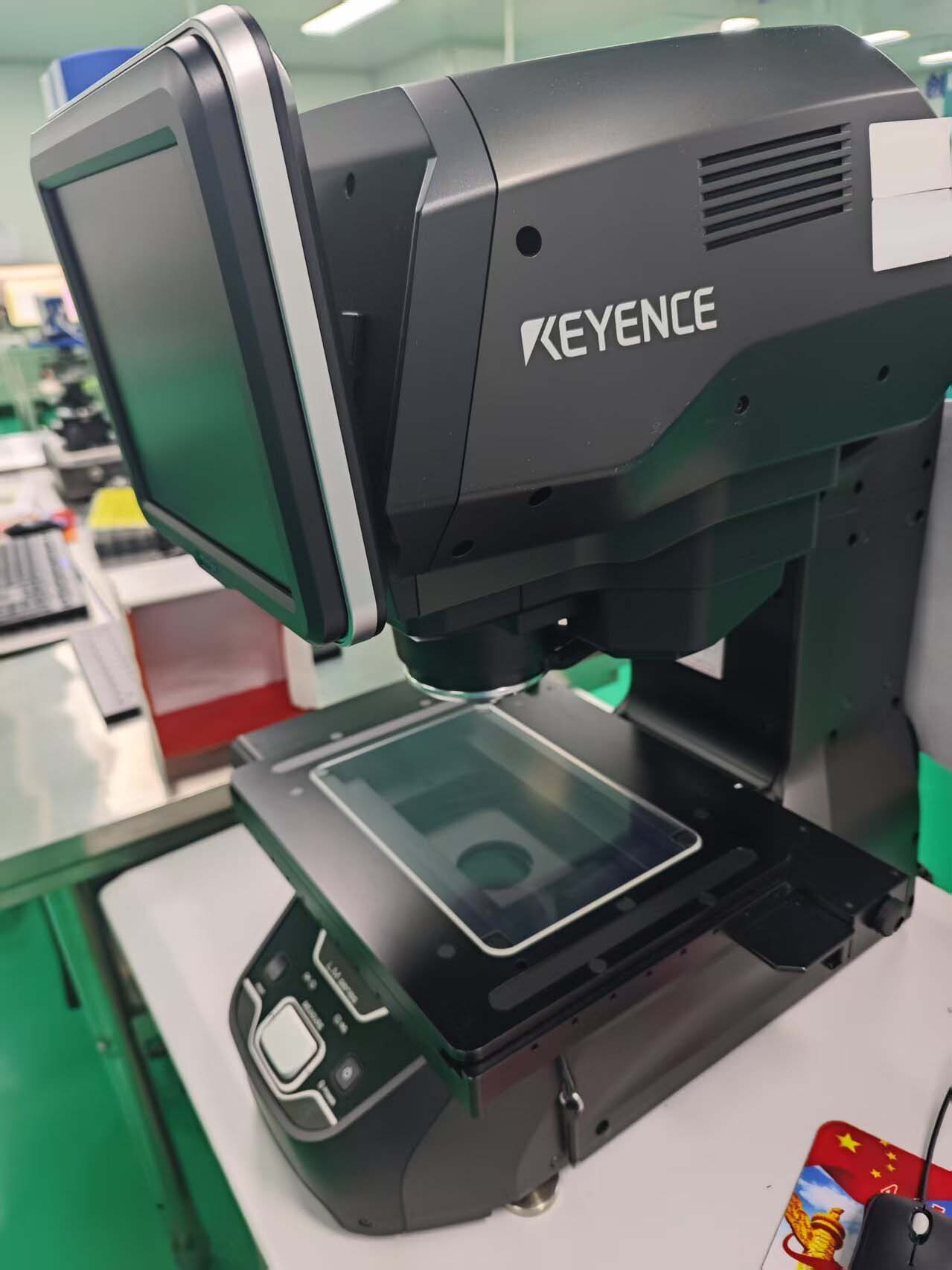

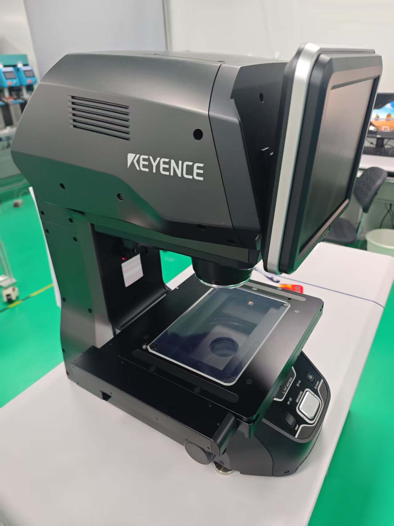
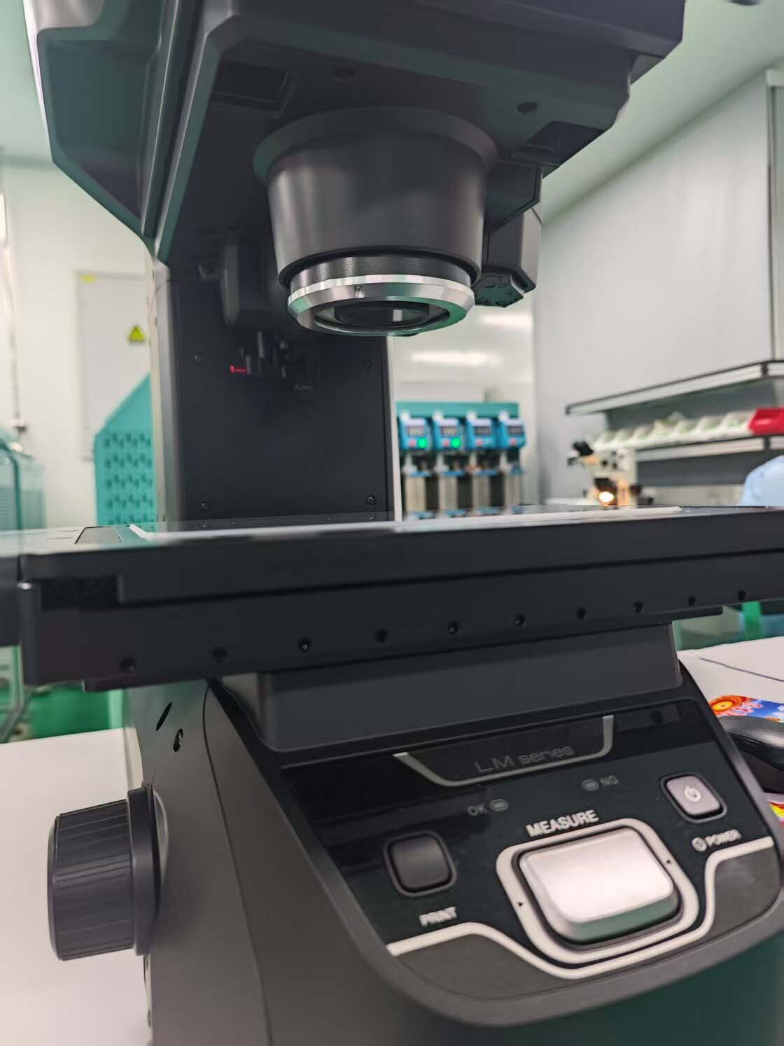
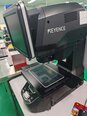
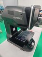
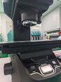
KEYENCE LM-1000 is a cutting-edge wafer testing and metrology equipment designed to provide high-precision, accurate, and efficient measurements for semiconductor manufacturing processes. With its advanced technology and features, LM-1000 offers unparalleled capabilities for ensuring the quality and reliability of semiconductor wafers used in various applications. One of the key features of KEYENCE LM-1000 is its high-speed and high-resolution imaging capabilities. The system is equipped with state-of-the-art cameras and sensors that can capture detailed images of semiconductor wafers with exceptional clarity and accuracy. This allows for precise measurements of critical parameters such as dimensions, defects, and surface roughness, enabling manufacturers to identify and address any issues that may affect the performance of the wafers. LM-1000 also offers advanced image processing and analysis algorithms that enhance the quality and reliability of the measurement data. These algorithms can automatically detect and classify defects, anomalies, and irregularities on the wafer surface, providing valuable insights into the quality of the semiconductor materials and the manufacturing process. By leveraging these advanced capabilities, manufacturers can optimize their production processes and improve the overall quality of their products. In addition to its imaging capabilities, KEYENCE LM-1000 is equipped with a range of metrology tools that enable precise and accurate measurements of critical parameters on semiconductor wafers. The unit features advanced measurement algorithms and software that can analyze various aspects of the wafer, including dimensions, thickness, flatness, and alignment, with exceptional accuracy and repeatability. This allows manufacturers to validate the quality of their wafers and ensure compliance with industry standards and specifications. Moreover, LM-1000 offers a user-friendly interface and intuitive software that make it easy for operators to set up, configure, and run measurements on the machine. The tool supports automated measurement routines and workflows, allowing for fast and efficient data acquisition and analysis. Operators can easily customize measurement settings, generate reports, and track quality metrics using the intuitive software interface, enhancing productivity and efficiency in semiconductor manufacturing operations. KEYENCE LM-1000 is also designed to be highly versatile and adaptable to a wide range of semiconductor manufacturing applications. The asset can accommodate various wafer sizes, materials, and geometries, making it suitable for use in diverse production environments. Whether measuring critical dimensions on silicon wafers, analyzing defects on compound semiconductor substrates, or characterizing thin film coatings on gallium nitride wafers, LM-1000 provides the flexibility and performance required for demanding semiconductor manufacturing processes. Overall, KEYENCE LM-1000 sets a new standard in wafer testing and metrology with its advanced imaging capabilities, precise measurement tools, user-friendly interface, and versatile design. By leveraging the capabilities of this innovative model, semiconductor manufacturers can improve the quality, efficiency, and reliability of their production processes, ultimately leading to enhanced product performance and customer satisfaction in the competitive semiconductor industry.
There are no reviews yet