Used KEYENCE LM-1100 #293766738 for sale
URL successfully copied!
Tap to zoom
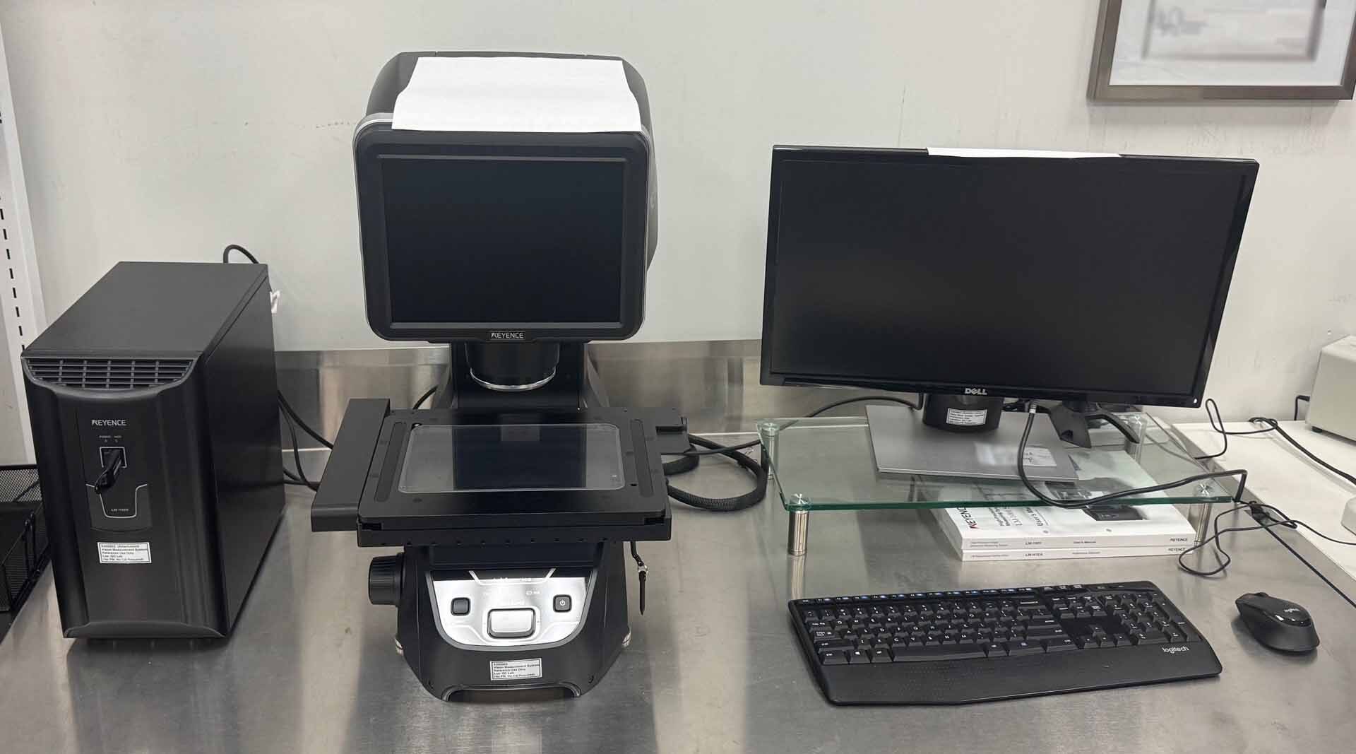

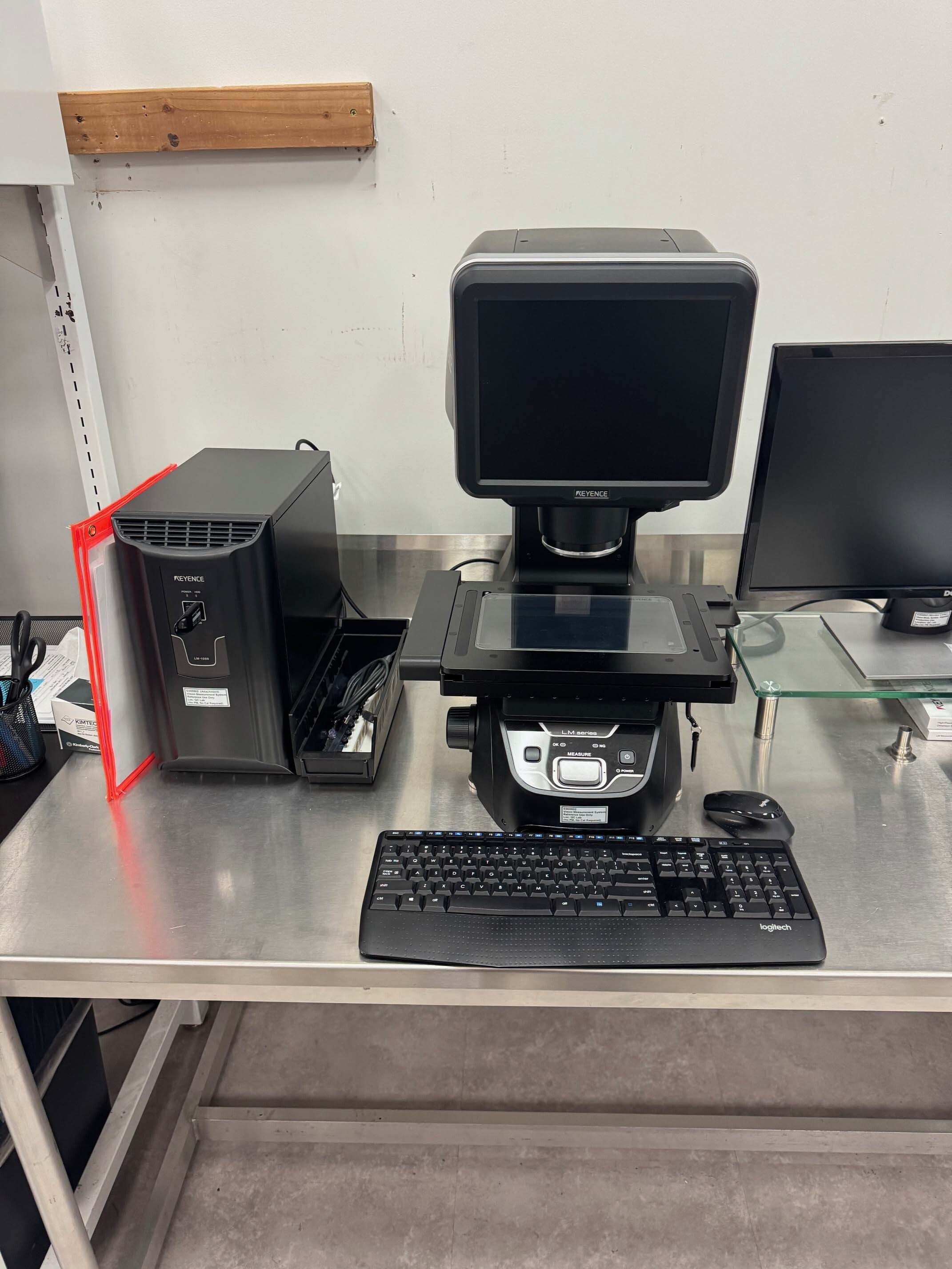
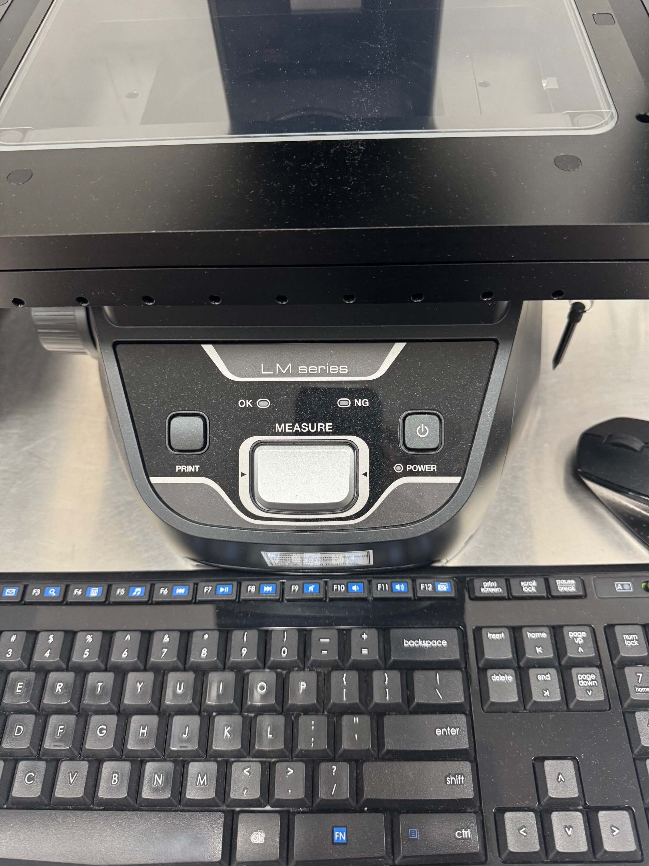
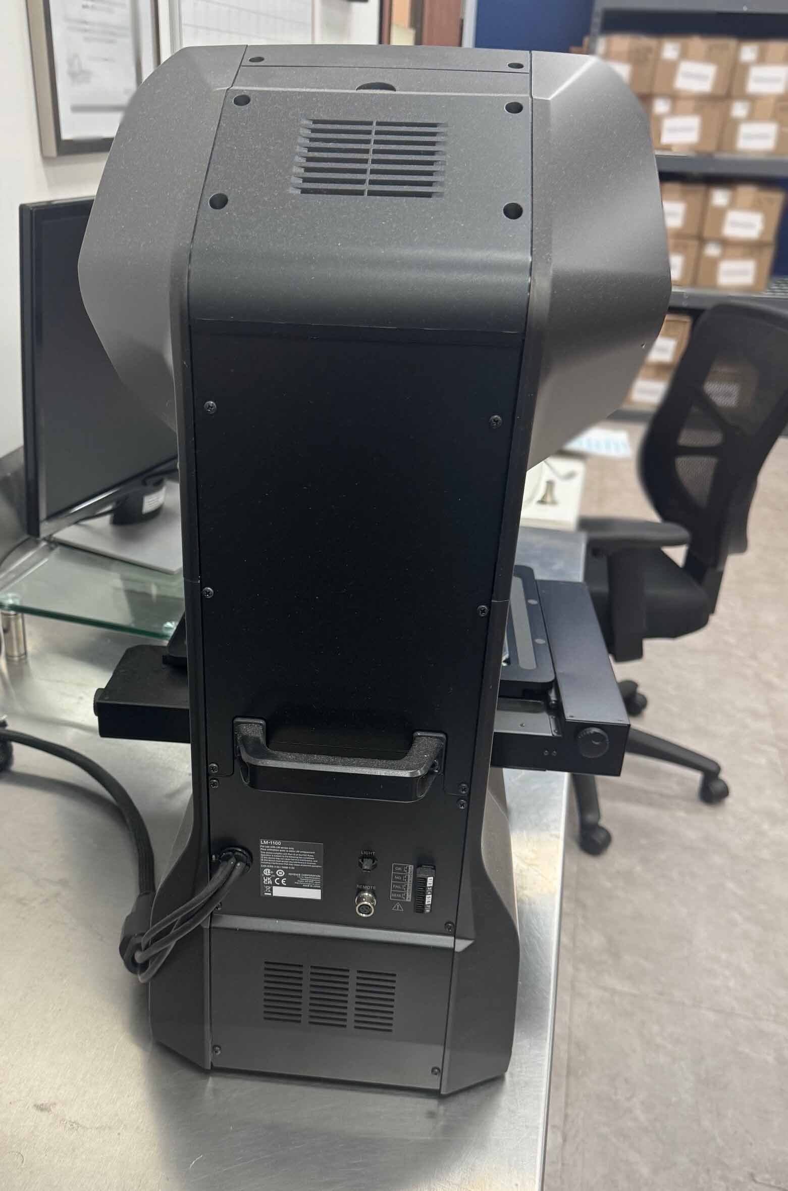
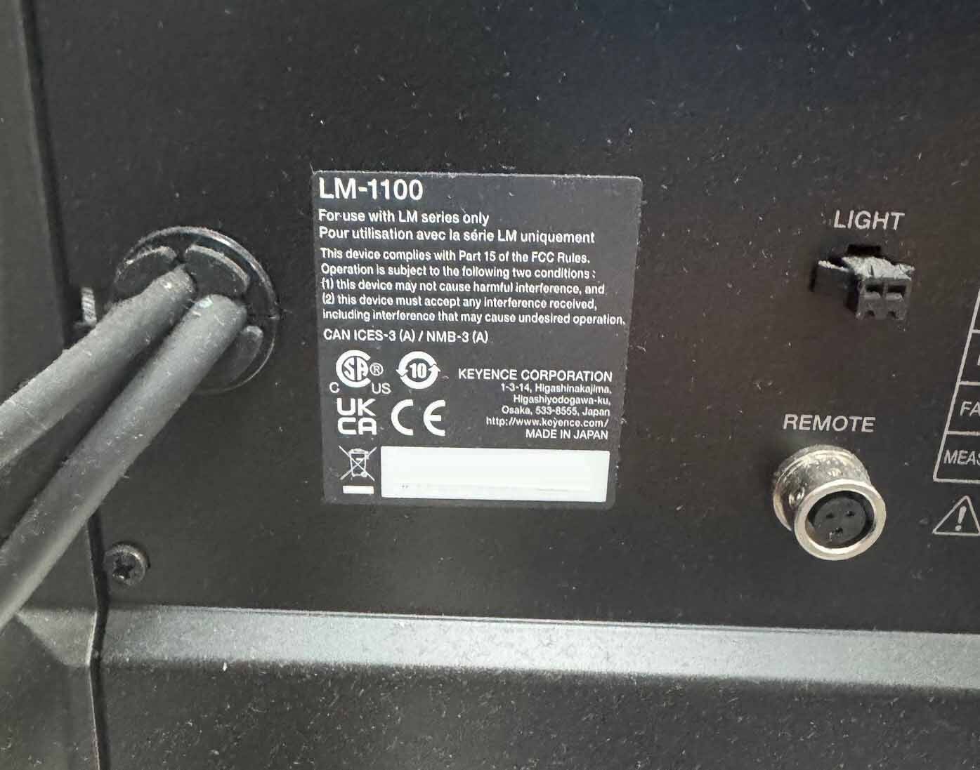
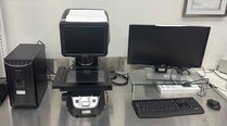
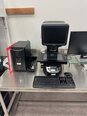
KEYENCE LM-1100 is an advanced wafer testing and metrology equipment designed for high-precision measurement and inspection of semiconductor wafers. This state-of-the-art system incorporates cutting-edge technologies to ensure accurate and reliable characterization of semiconductor devices, enabling manufacturers to achieve higher yields and improve overall production quality. One of the key features of LM-1100 is its automated wafer handling unit, which allows for rapid and efficient loading and unloading of wafers. This significantly reduces the time required for testing and measurement processes, increasing throughput and overall productivity. The machine is compatible with various wafer sizes, making it versatile and suitable for a wide range of semiconductor production applications. KEYENCE LM-1100 utilizes advanced optical technologies to perform non-destructive and high-resolution measurements of critical wafer parameters such as thickness, flatness, roughness, and defect detection. The tool is equipped with a high-speed scanning capability and intelligent image processing algorithms, enabling the accurate identification and classification of defects on the wafer surface. This allows manufacturers to quickly identify and address issues that may impact the final product quality. Furthermore, LM-1100 features a user-friendly interface with intuitive software that offers real-time visualization of measurement results and data analysis. The asset provides comprehensive metrology reports and statistical data analysis tools, allowing operators to gain valuable insights into wafer quality and process performance. This enables manufacturers to optimize production processes, troubleshoot issues, and make informed decisions to improve overall yield and quality control. In addition to its advanced measurement capabilities, KEYENCE LM-1100 is designed with a focus on reliability and durability. The model is built with high-quality components and materials, ensuring consistent and accurate performance over time. Its robust design and construction make it suitable for use in demanding semiconductor manufacturing environments, where precision and repeatability are critical requirements. Moreover, LM-1100 offers a range of customization options and accessories to meet specific industry needs and requirements. The equipment can be integrated with other semiconductor production equipment, such as automated wafer handling robots and inspection systems, to create a seamless and efficient production workflow. This flexibility allows manufacturers to tailor the system to their unique production processes and enhance overall operational efficiency. Overall, KEYENCE LM-1100 is a cutting-edge wafer testing and metrology unit that offers advanced measurement capabilities, robust performance, and user-friendly operation. Its features and capabilities make it an ideal solution for semiconductor manufacturers looking to achieve high yields, improve process control, and enhance the quality of their products.
There are no reviews yet