Used KEYENCE LM-1100 #293807814 for sale
URL successfully copied!



Tap to zoom
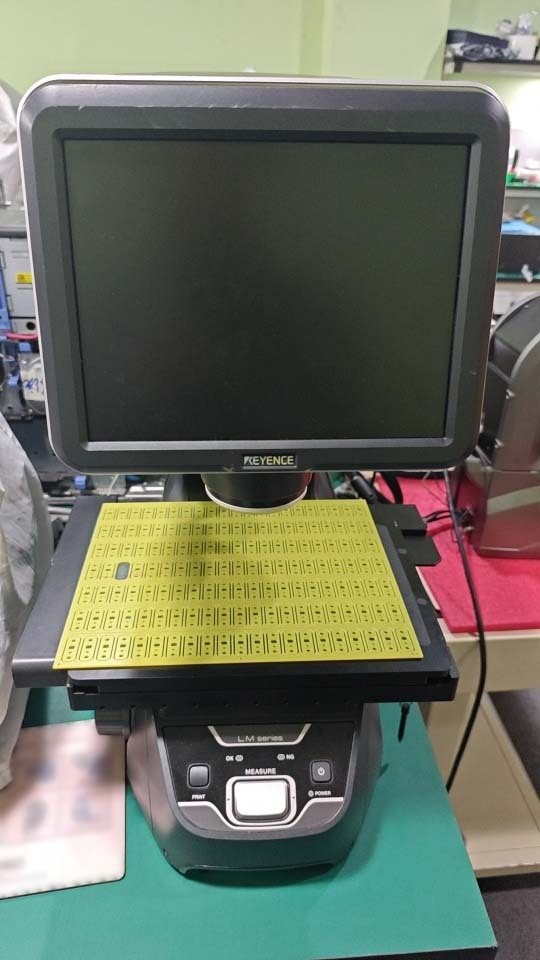

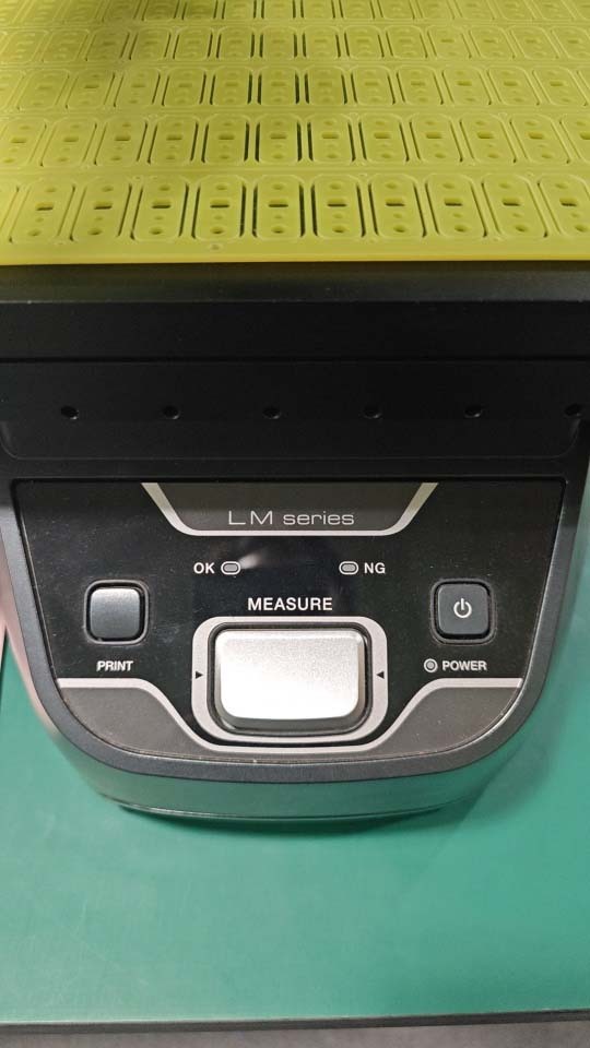
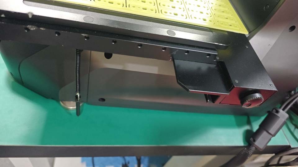
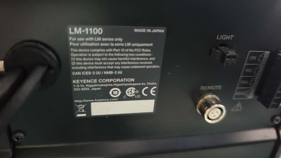
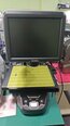
KEYENCE LM-1100 is an advanced wafer testing and metrology equipment specifically designed for semiconductor manufacturing applications. This cutting-edge system integrates various technologies and features to provide high-precision measurements and analysis of semiconductor wafers, enabling manufacturers to improve quality control, efficiency, and overall production yield. LM-1100 is equipped with a range of innovative optical and image processing technologies, including high-resolution cameras, advanced image sensors, and precision optics. These components work together to capture detailed images of the wafer surface with exceptional clarity and accuracy. The unit utilizes sophisticated algorithms and image processing techniques to analyze these images and extract crucial information about the wafer's geometry, surface quality, and defect characteristics. One of the key capabilities of KEYENCE LM-1100 is its ability to perform comprehensive dimensional measurements of semiconductor wafers with micron-level accuracy. The machine can accurately measure various parameters such as diameter, flatness, thickness, and alignment of features on the wafer surface. This precise dimensional measurement capability is essential for ensuring that the wafers meet strict specifications and quality standards required for semiconductor fabrication processes. In addition to dimensional measurements, LM-1100 is also capable of detecting and classifying defects on the wafer surface. The tool uses advanced image analysis algorithms to identify various types of defects, such as scratches, particles, pits, and other surface abnormalities. By accurately categorizing and quantifying these defects, manufacturers can identify potential quality issues early in the production process and take corrective actions to prevent yield loss and ensure product reliability. Furthermore, KEYENCE LM-1100 offers advanced metrology capabilities for characterizing the topography and roughness of the wafer surface. The asset can generate detailed 3D surface maps and profiles, providing valuable insights into the wafer's surface morphology and texture. This information is critical for optimizing wafer processing steps, such as lithography and etching, to achieve precise patterning and device performance. LM-1100 is designed to streamline wafer inspection and metrology workflows in semiconductor manufacturing facilities. The model features a user-friendly interface and intuitive software that allows operators to easily set up inspections, customize measurement recipes, and analyze data efficiently. The equipment supports automated wafer handling and positioning, enabling rapid throughput and high productivity for mass production environments. Moreover, KEYENCE LM-1100 offers seamless integration with other manufacturing equipment and software systems through industry-standard communication protocols. This interoperability allows manufacturers to incorporate the system into their existing production line and data management infrastructure, enhancing overall process efficiency and data traceability. In conclusion, LM-1100 is a state-of-the-art wafer testing and metrology unit that empowers semiconductor manufacturers to achieve superior quality control and process optimization. With its advanced imaging technologies, precise measurements, defect detection capabilities, and user-friendly interface, KEYENCE LM-1100 is a versatile solution for enhancing yield, reliability, and performance in semiconductor fabrication.
There are no reviews yet