Used KEYENCE LM-1100 #293814077 for sale
URL successfully copied!
Tap to zoom
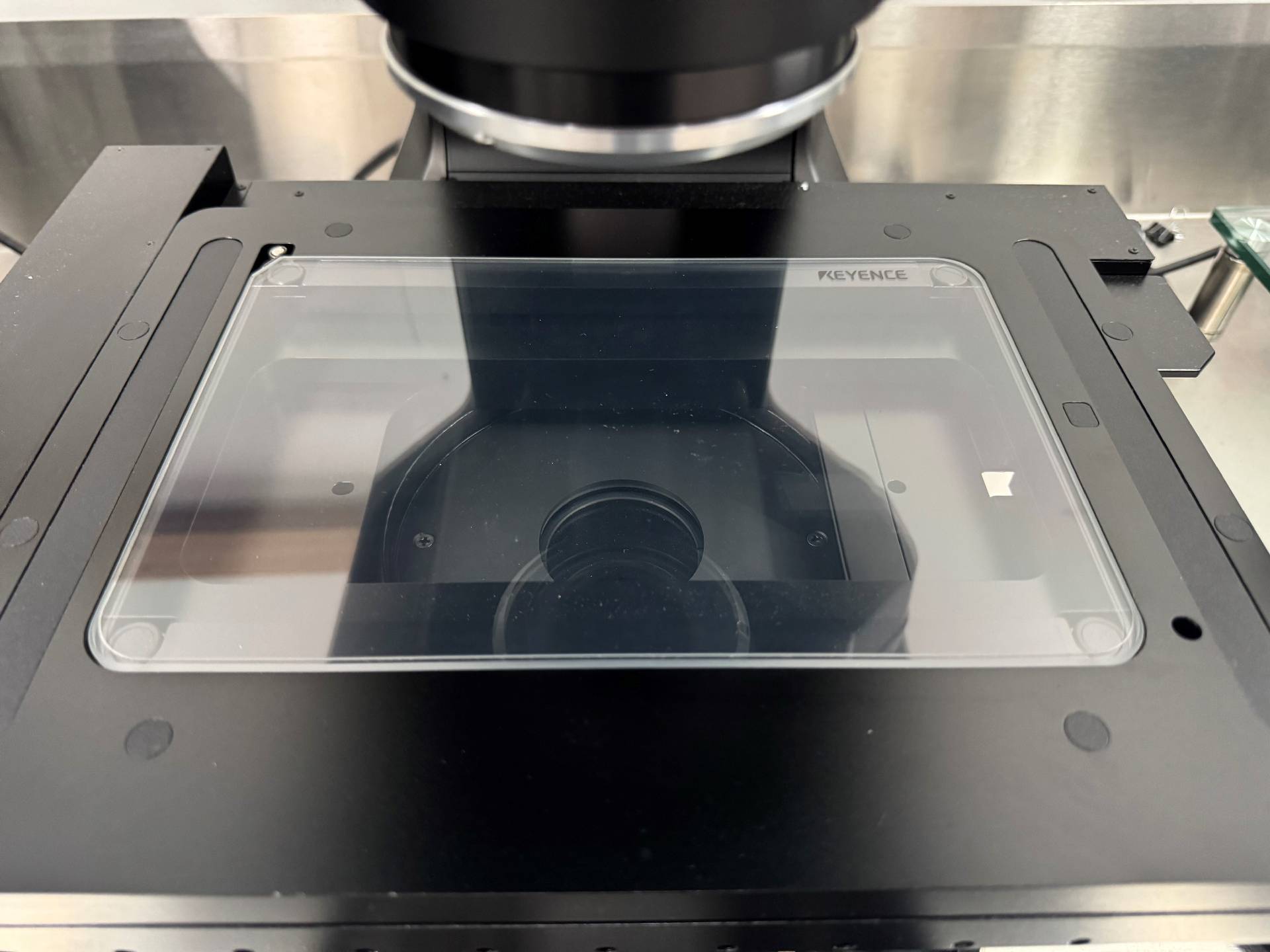

KEYENCE LM-1100 is a cutting-edge wafer testing and metrology equipment designed to provide precise and efficient measurement solutions for semiconductor manufacturing processes. This advanced system incorporates a range of innovative technologies and features tailored to meet the demanding requirements of the semiconductor industry. At the core of LM-1100 unit is its high-precision measurement capabilities, which enable accurate and repeatable characterization of wafer samples. The machine incorporates advanced optical sensors and imaging technology to capture detailed information about the physical and chemical properties of the wafers. This information is then used to perform critical measurements such as thickness, flatness, roughness, and defect detection with exceptional accuracy. One key feature of KEYENCE LM-1100 tool is its non-contact measurement methodology, which eliminates the risk of damage to delicate wafer samples during testing. The asset utilizes advanced laser and optics technology to obtain measurement data without physical contact with the wafer surface, ensuring that the integrity of the samples is preserved throughout the testing process. LM-1100 model is also equipped with a sophisticated automation capability that enables high throughput testing of wafers. The equipment can be seamlessly integrated into semiconductor manufacturing lines, allowing for continuous and efficient wafer testing operations. This automation capability is further enhanced by intelligent software algorithms that optimize the testing process and minimize the need for manual intervention. In addition to its measurement and automation features, KEYENCE LM-1100 system offers a range of advanced analysis tools for wafer metrology. These tools include powerful data processing algorithms that extract meaningful insights from the measurement data and characterize critical wafer parameters. The unit also provides comprehensive visualization capabilities, allowing users to analyze and interpret measurement results with ease. Another key aspect of LM-1100 machine is its versatility and adaptability to different wafer sizes and types. The tool supports a wide range of wafer materials, including silicon, compound semiconductors, and other exotic materials used in semiconductor manufacturing. It also offers flexibility in terms of wafer size compatibility, allowing for testing of wafers with varying diameters and thicknesses. Furthermore, KEYENCE LM-1100 asset is designed with user-friendly features and intuitive interfaces to facilitate ease of operation and streamline the testing process. The model can be easily configured and calibrated by operators, minimizing setup time and ensuring consistent and reliable measurement results. Overall, LM-1100 wafer testing and metrology equipment represents a state-of-the-art solution for semiconductor manufacturers seeking precision, efficiency, and reliability in their wafer testing processes. With its advanced measurement capabilities, automation features, and versatility, the system is well-suited to meet the evolving needs of the semiconductor industry and drive innovation in wafer characterization and quality control.
There are no reviews yet