Used KEYENCE LM-1100 #293819792 for sale
URL successfully copied!

Tap to zoom
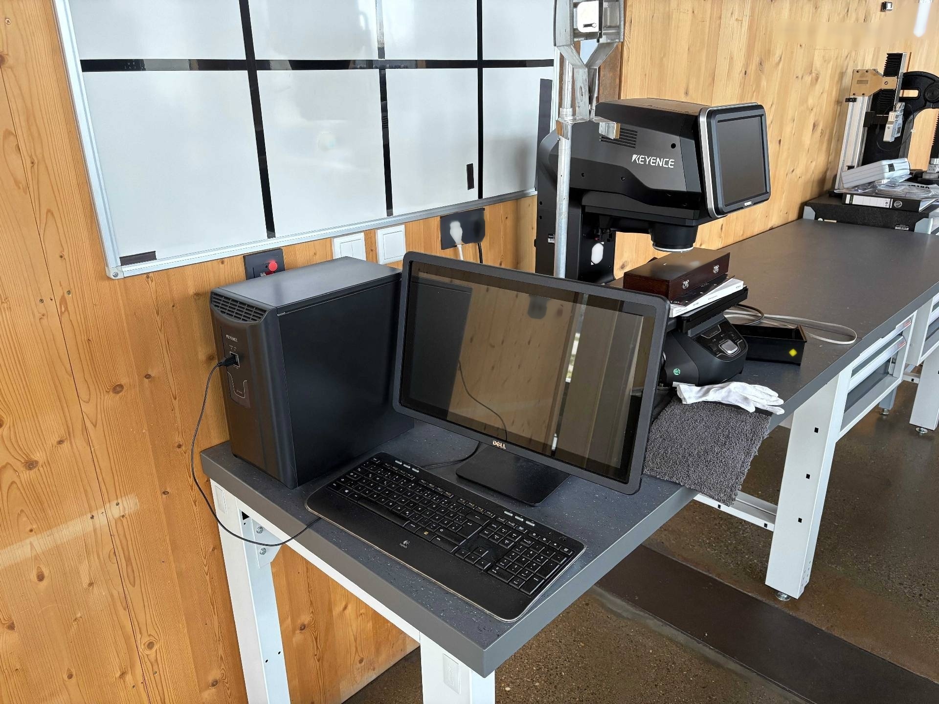

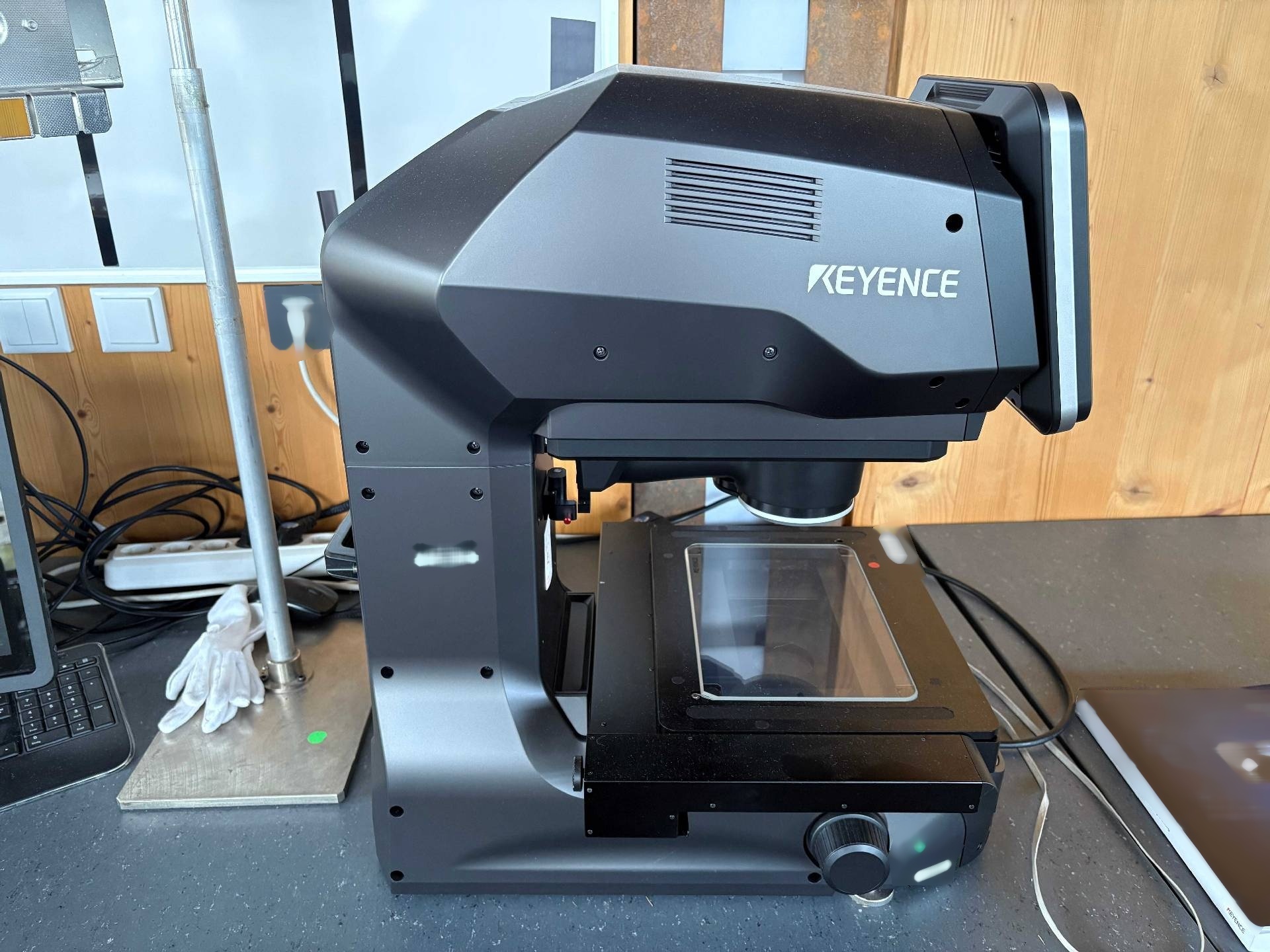
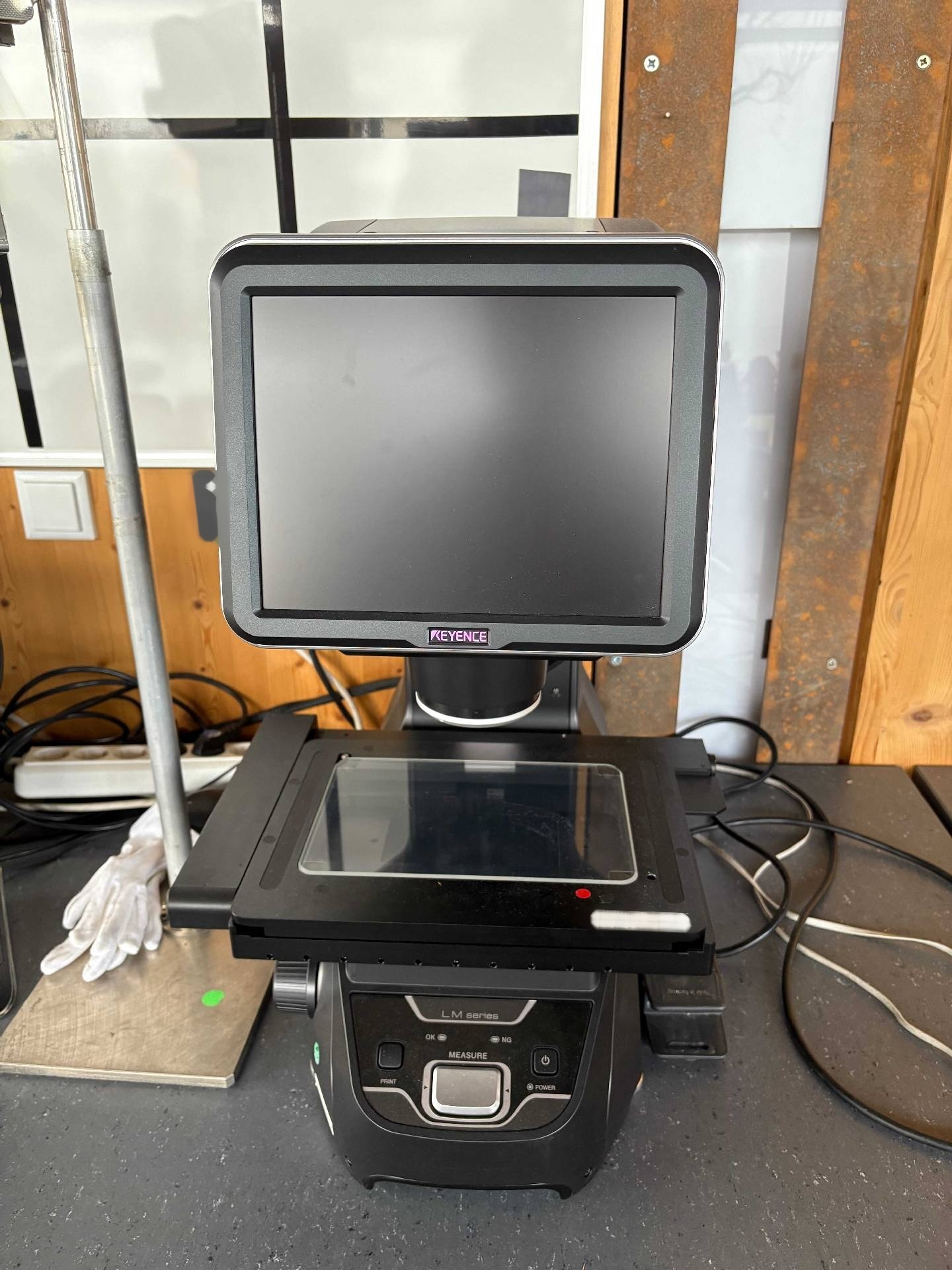
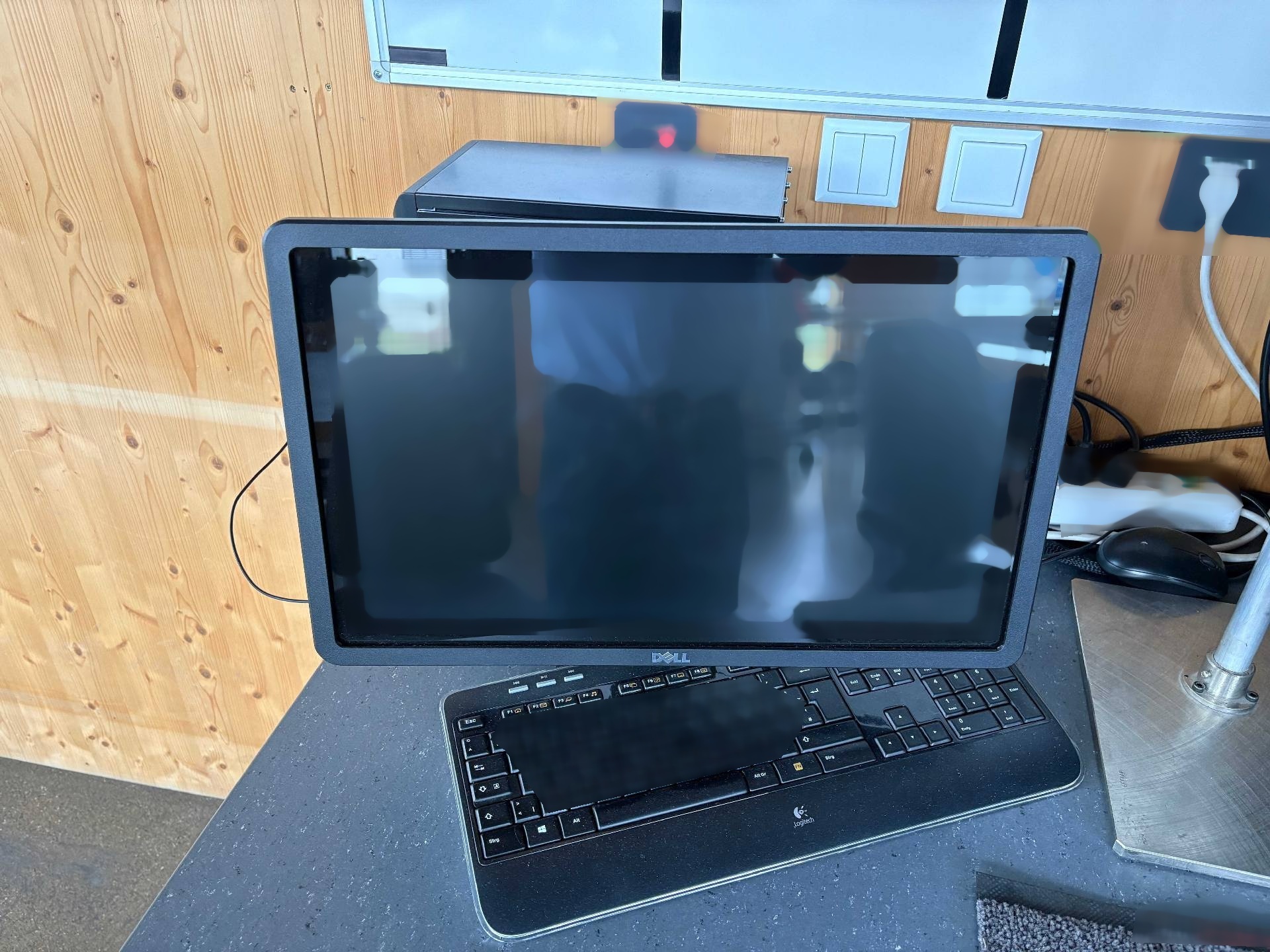
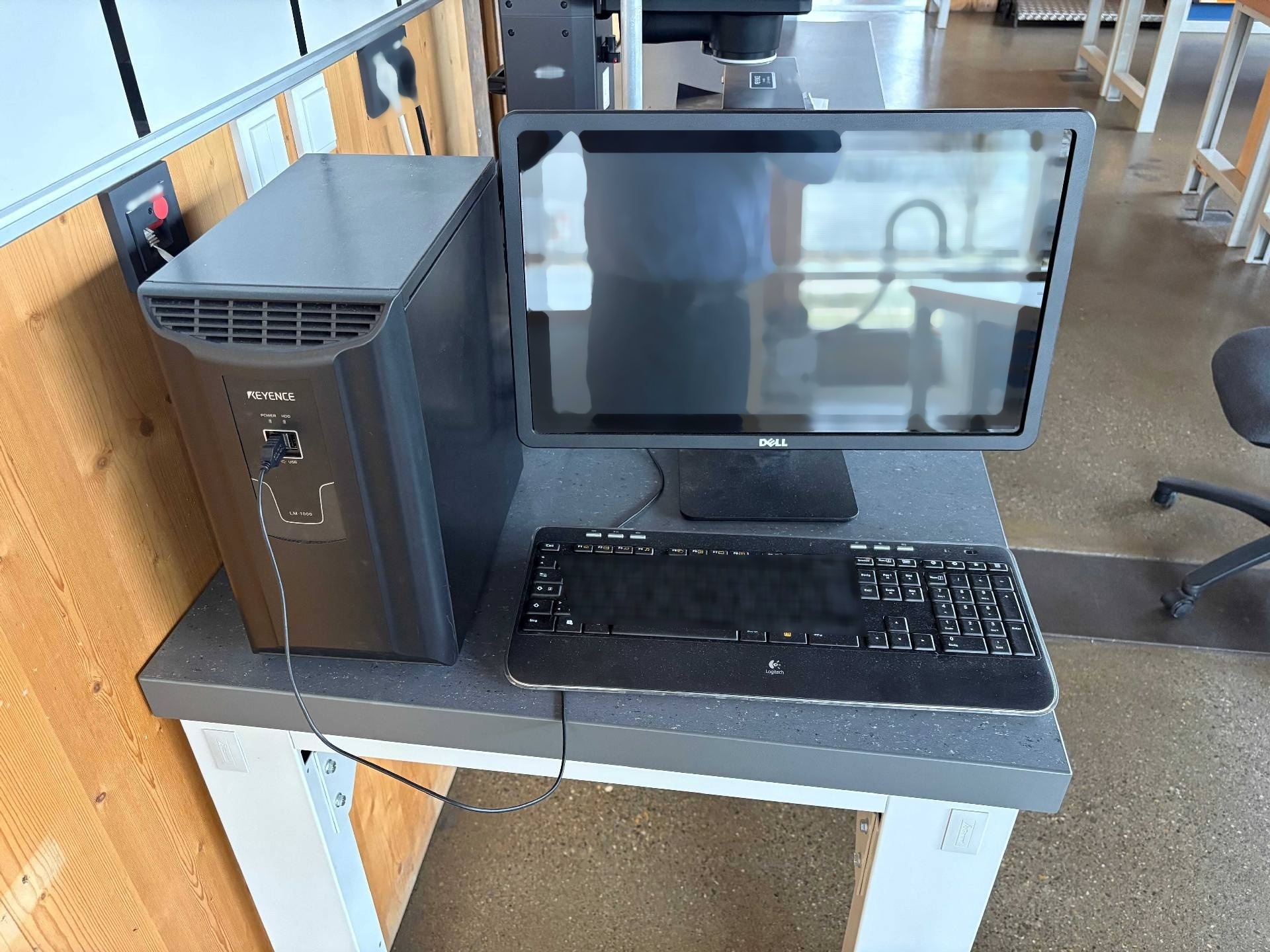
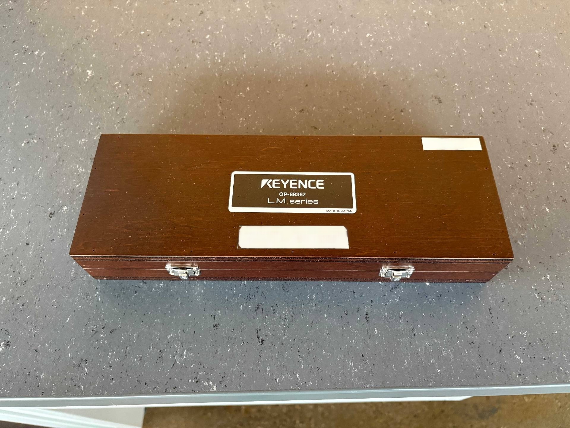
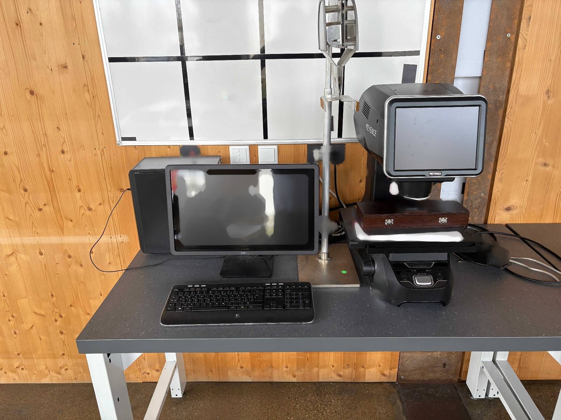
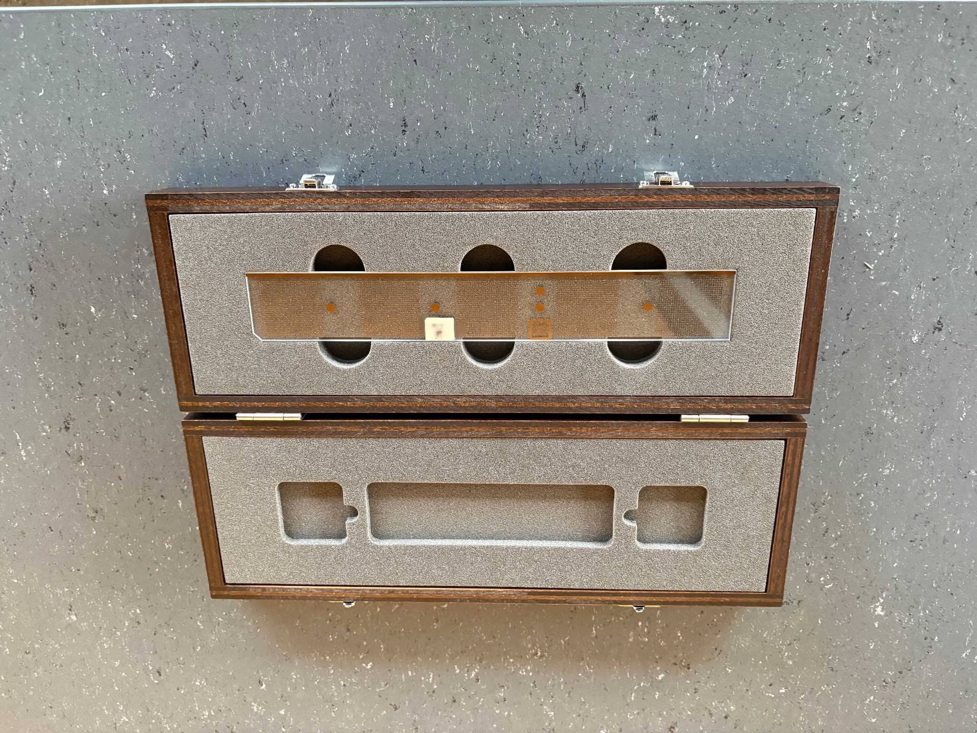
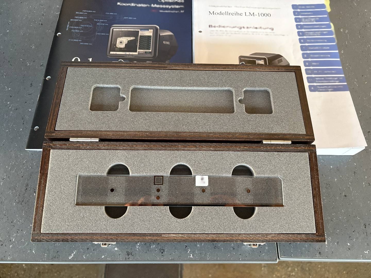
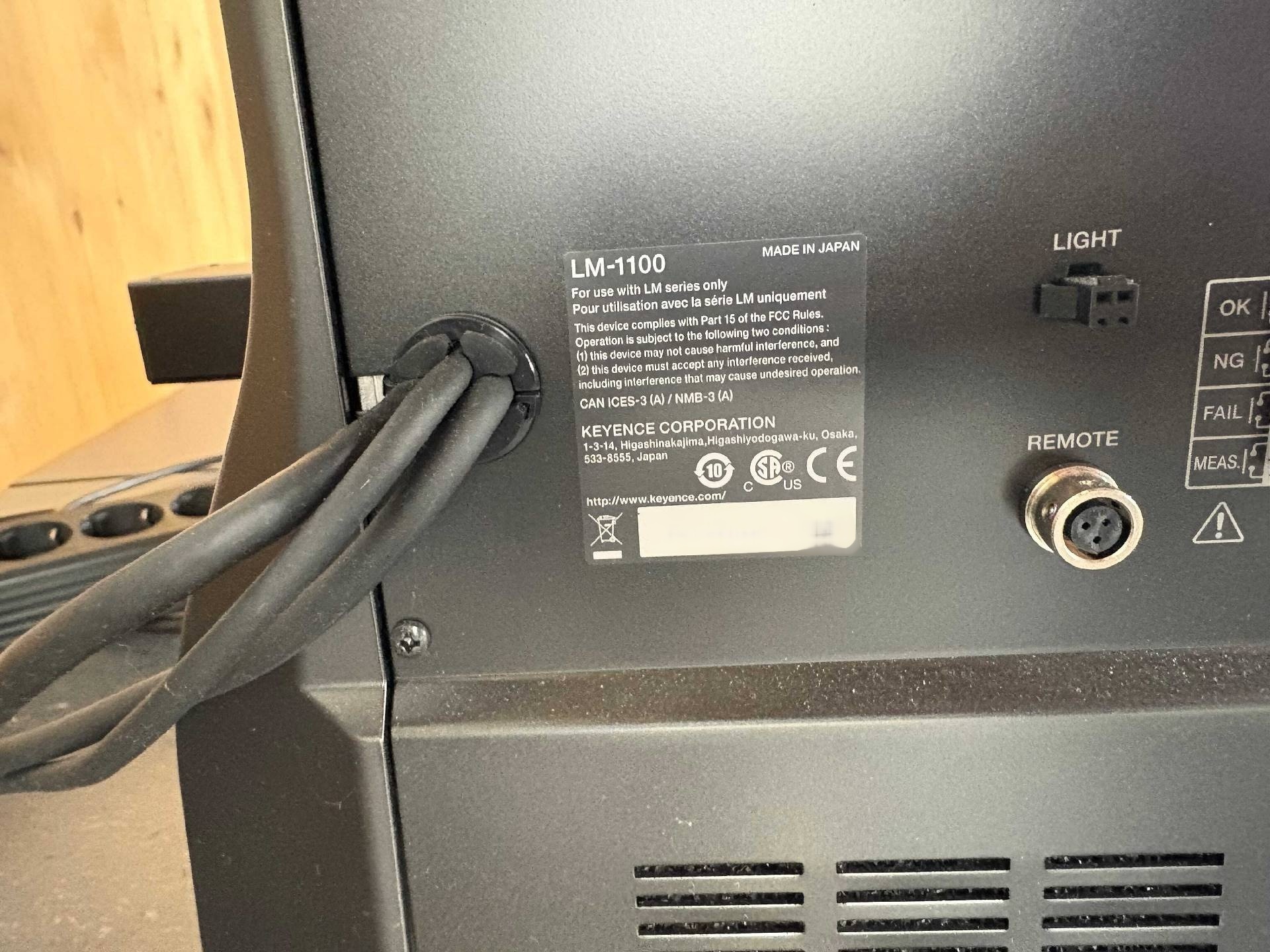
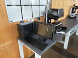
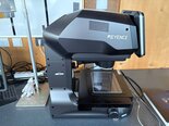
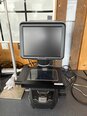
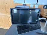
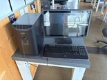
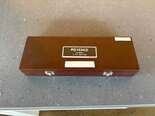
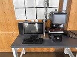
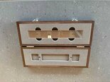
KEYENCE LM-1100 is a cutting-edge wafer testing and metrology equipment that addresses the stringent requirements of the semiconductor industry by offering high precision, advanced features, and comprehensive measurement capabilities. Leveraging the latest technologies and innovations in the field, this system delivers accurate and reliable results for the characterization and optimization of semiconductor wafers. At the core of LM-1100 is its advanced optical measurement capabilities, which enable high-resolution imaging and precise dimensional analysis of semiconductor wafers. The unit is equipped with a powerful microscope that offers magnification options for detailed inspection of wafer features at the micro and nano scales. This allows for the detection of defects, pattern deviations, and other imperfections that can impact semiconductor device performance. The machine also features advanced image processing algorithms that enhance the visibility and clarity of wafer images, making it easier to identify and analyze critical features. These algorithms help in the automatic detection and classification of defects, reducing the time and effort required for manual inspection tasks. Additionally, the tool's software provides intuitive tools for data visualization, analysis, and reporting, enabling users to make informed decisions based on the collected measurement data. In terms of measurement capabilities, KEYENCE LM-1100 offers a wide range of options for characterizing semiconductor wafers. It can perform measurements of critical dimensions, thickness, roughness, flatness, and other parameters with high accuracy and repeatability. The asset supports various measurement modes, including brightfield and darkfield imaging, confocal microscopy, and 3D profiling, allowing for comprehensive analysis of wafer properties. Moreover, LM-1100 is equipped with automated measurement routines that streamline the testing process and improve productivity. The model can perform multi-point measurements, scan large areas of the wafer surface, and generate detailed maps of wafer properties, all with minimal user intervention. This automation reduces human errors, enhances measurement consistency, and speeds up the overall testing workflow. In terms of connectivity and integration, KEYENCE LM-1100 is designed to seamlessly interface with other equipment and systems commonly used in semiconductor manufacturing environments. It supports industry-standard communication protocols for data exchange and can be integrated into larger production lines for inline testing and metrology applications. The equipment's software also allows for easy data transfer, storage, and sharing, facilitating collaboration and data management within semiconductor facilities. Overall, LM-1100 is a state-of-the-art wafer testing and metrology system that offers unmatched capabilities for the characterization and optimization of semiconductor wafers. With its advanced optical measurement technologies, automated features, and comprehensive analysis tools, this unit is a valuable asset for semiconductor manufacturers seeking to ensure the quality and reliability of their products.
There are no reviews yet