Used KEYENCE LM-1100 #293821240 for sale
URL successfully copied!
Tap to zoom
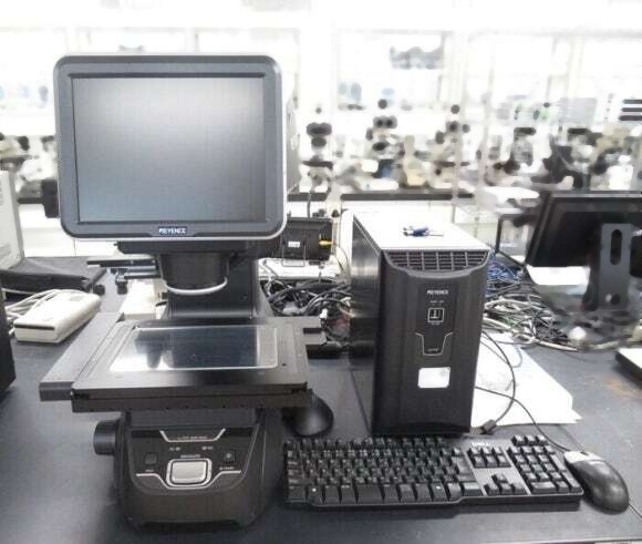

KEYENCE LM-1100 is a highly advanced wafer testing and metrology equipment designed to meet the demanding requirements of semiconductor manufacturing processes. This system offers cutting-edge technology and superior performance for accurate and efficient measurement and inspection of wafers used in the fabrication of integrated circuits and other semiconductor devices. LM-1100 is equipped with a range of innovative features that enable high-speed and high-precision testing of wafers, thereby ensuring the quality and reliability of the semiconductor products. One of the key features of this unit is its multi-sensor technology, which combines multiple measurement techniques such as confocal microscopy, white light interferometry, and laser displacement sensors to provide comprehensive and detailed analysis of the wafer surface topography and characteristics. The confocal microscopy feature of KEYENCE LM-1100 allows for non-contact, three-dimensional imaging of the wafer surface with high resolution and accuracy. This technology utilizes a scanning laser beam to directly measure the height profile of the wafer features, enabling precise detection of defects, particles, and other surface abnormalities that may impact the performance of the semiconductor devices. In addition to confocal microscopy, LM-1100 incorporates white light interferometry for precise measurement of surface roughness, step heights, and film thickness on the wafer surface. This technique uses the interference patterns generated by white light to accurately determine the height differences between different features on the wafer, offering valuable insights into the quality and uniformity of the semiconductor materials. Furthermore, the laser displacement sensors integrated into KEYENCE LM-1100 provide rapid and accurate measurement of flatness, thickness, and other critical parameters of the wafers. These sensors emit a laser beam onto the wafer surface and detect the reflected light to determine the distance between the sensor and the wafer, enabling real-time monitoring of the wafer profile and ensuring compliance with the stringent specifications of the semiconductor industry. LM-1100 also features advanced image processing algorithms and data analysis software that enable automated inspection and analysis of the measurement data acquired from the wafers. This software allows for intelligent defect detection, classification, and mapping, as well as statistical process control and trend analysis to optimize the manufacturing processes and enhance the overall efficiency and productivity of the semiconductor production line. Moreover, KEYENCE LM-1100 is designed for easy integration into existing semiconductor manufacturing environments, with a user-friendly interface and flexible data output options that streamline the data management and reporting processes. This machine is equipped with a robust and reliable hardware platform that ensures stable and accurate performance in the demanding conditions of semiconductor fabrication facilities. In conclusion, LM-1100 sets a new standard in wafer testing and metrology with its advanced multi-sensor technology, high-speed measurement capabilities, and sophisticated data analysis tools. This tool provides semiconductor manufacturers with a powerful tool for ensuring the quality and reliability of their products, improving process efficiency, and meeting the stringent requirements of the semiconductor industry.
There are no reviews yet