Used KEYENCE VR-3000 #293806466 for sale
URL successfully copied!

Tap to zoom
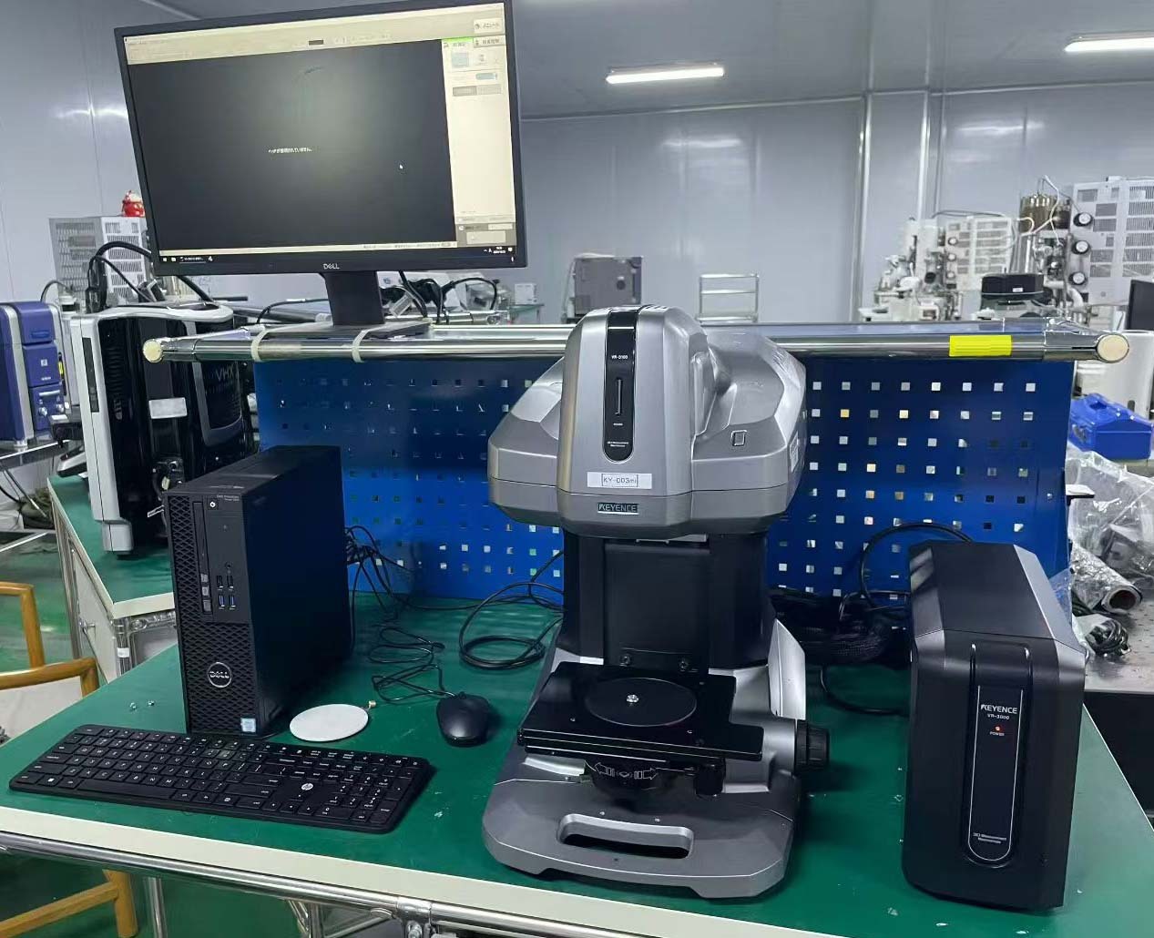

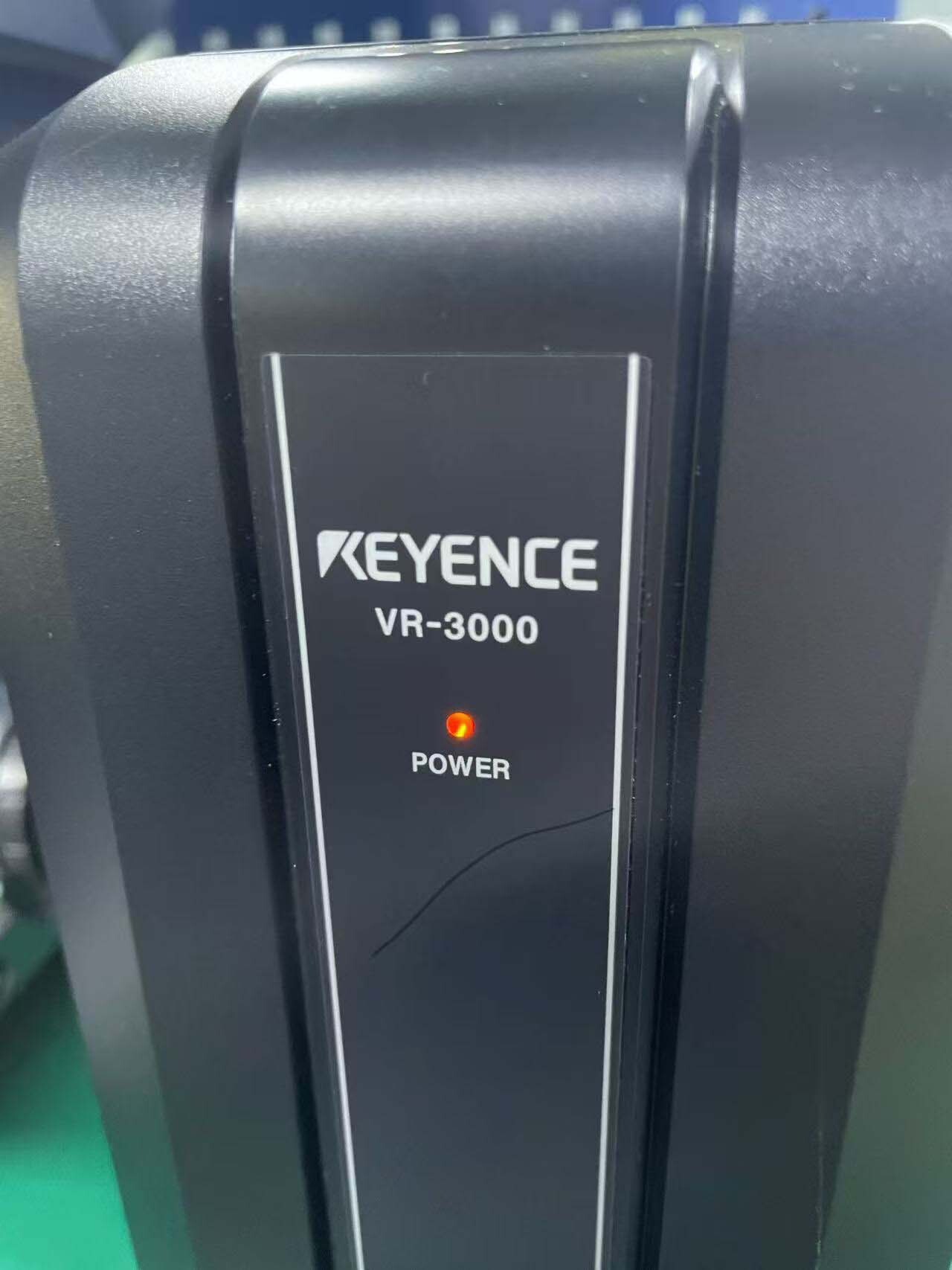
KEYENCE VR-3000 is a cutting-edge wafer testing and metrology equipment designed to provide high-precision measurement and analysis capabilities for semiconductor manufacturing processes. This advanced system integrates state-of-the-art technology to deliver accurate and reliable data for characterizing wafers, ensuring quality control, and optimizing production efficiency. At the core of VR-3000 is its sophisticated optical measurement technology, which utilizes advanced algorithms and image processing techniques to capture detailed information about the surface profile, morphology, and dimensions of wafers with exceptional precision. The unit is equipped with a high-resolution imaging sensor that can capture fine details and features on the wafer surface, enabling it to perform comprehensive inspections and measurements at the micrometer level. One of the key features of KEYENCE VR-3000 is its non-contact measurement capability, which eliminates the risk of damage or contamination to delicate semiconductor wafers during the testing process. By utilizing non-destructive optical techniques, the machine can scan wafers without physical contact, ensuring the integrity and quality of the samples remain intact throughout the testing procedure. This non-contact approach also enhances the tool's productivity by reducing setup time and minimizing maintenance requirements. Furthermore, VR-3000 is designed to support automated wafer handling and measurement tasks, streamlining the testing process and increasing throughput in semiconductor manufacturing facilities. The asset is equipped with robotic arms, wafer mapping algorithms, and advanced software controls that enable it to perform rapid and precise measurements on multiple wafers in a high-throughput mode, improving overall productivity and operational efficiency. Another key capability of KEYENCE VR-3000 is its advanced data analysis and visualization tools, which allow users to analyze and interpret measurement results with enhanced clarity and insight. The model generates detailed 3D models, surface roughness maps, and other visual representations of wafer characteristics, enabling users to identify defects, anomalies, and variations in the semiconductor materials with exceptional accuracy. In addition to its measurement and analysis capabilities, VR-3000 offers a range of customization options and software features that enable users to tailor the equipment to specific requirements and applications in semiconductor manufacturing. The system can be configured with different imaging modes, measurement parameters, and data processing algorithms to accommodate diverse wafer types, materials, and processing techniques, ensuring optimal performance and compatibility in various production environments. Overall, KEYENCE VR-3000 represents a state-of-the-art solution for wafer testing and metrology in semiconductor manufacturing, combining advanced optical technology, automation capabilities, and data analysis tools to enable precise, reliable, and efficient characterization of wafers. With its high-precision measurements, non-contact operation, and versatile customization options, the unit is a valuable asset for semiconductor companies seeking to achieve quality control, process optimization, and performance excellence in their manufacturing operations.
There are no reviews yet