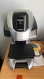
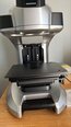
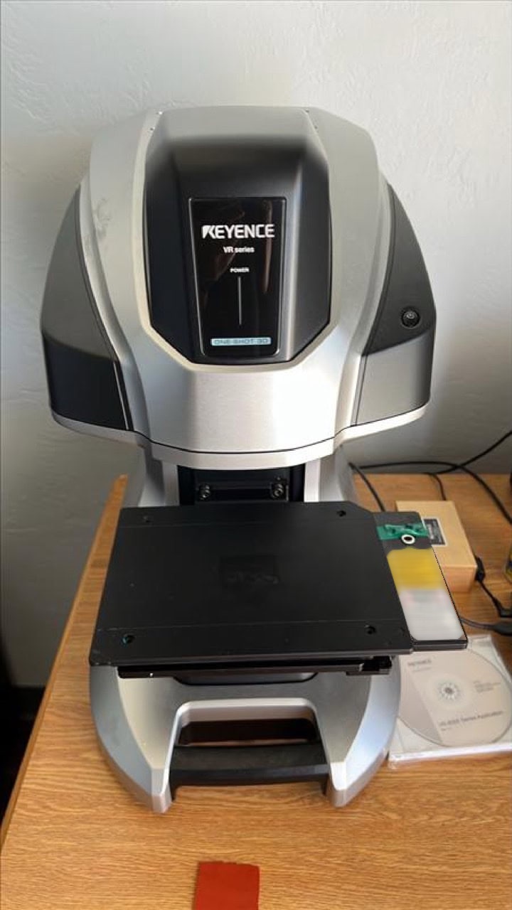
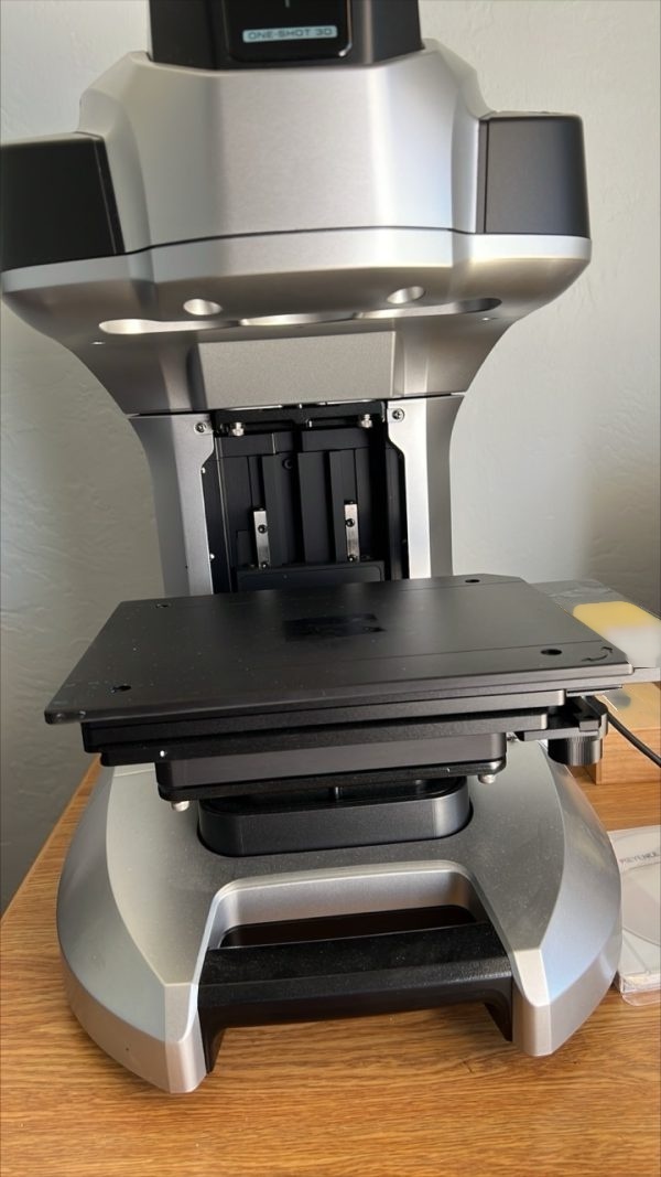
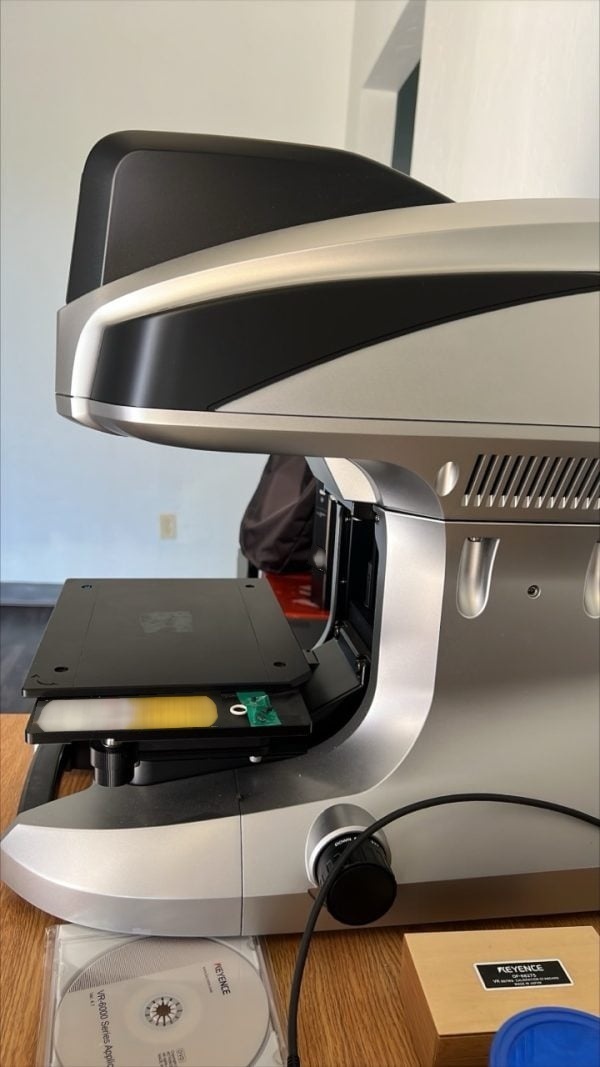
Used KEYENCE VR-6100 #293820293 for sale
URL successfully copied!
Tap to zoom

ID: 293820293
Vintage: 2021
3D optical profiler
Controller: VR-6000
4-megapixel monochrome Complementary Metal-Oxide-Semiconductor (CMOS)
(2) Double-telecentric lenses
Light-Emitting Diode (LED) observation light source
Personal Computer (PC)
Operating System (OS): Windows 10 Professional / Windows 11 Professional
2021 vintage.
KEYENCE VR-6100 is an advanced wafer testing and metrology equipment designed to meet the high demands of the semiconductor industry for precision, accuracy, and efficiency. This cutting-edge system incorporates innovative technology to provide comprehensive testing and measurement capabilities for wafer inspection and analysis in semiconductor manufacturing processes. One of the key features of VR-6100 is its advanced optical inspection unit, which utilizes high-resolution imaging technology to capture detailed images of the wafer surface. The machine is equipped with a high-speed camera and sophisticated image processing algorithms that allow for rapid and accurate detection of defects, particles, and other imperfections on the wafer. This enables users to perform comprehensive quality control checks and ensure the integrity of the semiconductor devices being manufactured. In addition to optical inspection, KEYENCE VR-6100 also offers advanced metrology capabilities for accurate measurement of critical dimensions on the wafer. The tool is equipped with precision measurement tools, such as laser displacement sensors and automated scanning mechanisms, to accurately capture dimensions, thicknesses, and profiles of various features on the wafer. This metrology functionality is essential for ensuring the dimensional accuracy and consistency of semiconductor devices, as even minor variations in dimensions can impact device performance and reliability. VR-6100 is designed for high-throughput semiconductor manufacturing environments, with a fast inspection and measurement capability that enables quick feedback to the production process. The asset features automated wafer handling mechanisms and sophisticated software algorithms that enable rapid data acquisition and analysis, reducing inspection times and increasing overall manufacturing efficiency. This high-speed performance is crucial for meeting the demanding production requirements of the semiconductor industry and ensuring timely delivery of high-quality semiconductor devices. Furthermore, KEYENCE VR-6100 is equipped with advanced data management and reporting functionalities to support comprehensive wafer traceability and documentation. The model automatically records inspection results, measurements, and other relevant data for each wafer, providing a detailed history of the manufacturing process and enabling quick identification of any deviations or issues. This data tracking capability is critical for quality control, process optimization, and compliance with industry standards and regulations. In conclusion, VR-6100 is a state-of-the-art wafer testing and metrology equipment that offers advanced inspection, measurement, and data management capabilities for semiconductor manufacturing. Its high-speed performance, precision accuracy, and comprehensive functionality make it a valuable tool for ensuring the quality and reliability of semiconductor devices, optimizing production processes, and meeting the stringent requirements of the semiconductor industry. With its advanced technology and innovative features, KEYENCE VR-6100 is a versatile and powerful solution for wafer inspection and metrology in semiconductor manufacturing applications.
There are no reviews yet