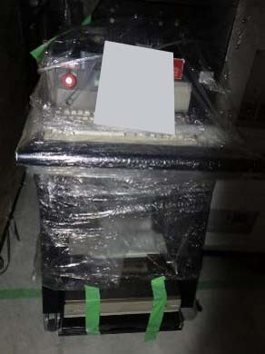
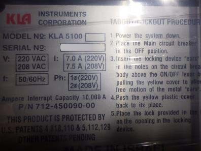
Used KLA / TENCOR 5100 XP #293727707 for sale
URL successfully copied!
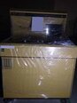
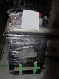
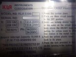
Tap to zoom
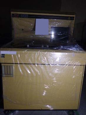

ID: 293727707
Wafer Size: 8"
Vintage: 1996
Overlay measurement system, 8"
Wafer loader system:
Transport system: (2) Cassette loader / unloader
Pre-alignment: OF Detection function
Control console:
Menu terminal
Image display terminal
5501 Analysis station
DEC VLC 4000
RAM: 16 MB
QIC Tape drive: 320/525 MB
Floppy Disk Drive: 3.5"
Image hard copy
Printer
SECS
Patlite
Hard Disk Drive (HDD): 2 GB
Wafer thickness: 725 µm
Minimum die size: 3 mm
Maximum die size: 50 mm
Measurement throughput: <85 Sheets / hour
Clean dry air:
Flow rate: 84.9 l/min
Pressure 603 kg/cm² - 7.7 kg/cm²
Tube, 1/4"
(3) Vacuums:
Hg: 635 mm
Flow rate: 28.3 l/min
Tube, 1/4"
Exhaust:
Duct system: 14.5"
Flow rate: 250 cfm
Missing parts
Temperature: 19°C - 25°C
Power supply: 200 VAC, 20 A, Single phase, 50/60 Hz
1996 vintage.
KLA / TENCOR 5100 XP is a highly advanced wafer testing and metrology equipment designed for use in high-end research and development laboratories. The system uses advanced spectroscopy technologies to measure the physical properties of wafers. The unit provides accurate measures of such parameters as optical and electrical resistivity, microstructure, and film thickness, enabling researchers to optimise the manufacture of cutting-edge microelectronic products. The machine features a powerful inspection tool, capable of imaging wafers within a 12-inch diameter, with accuracy and sensitivity to 0.1 micrometres. Additionally, the asset can rapidly scan and analyze the entire surface of a single wafer in less than a few minutes, making it an ideal choice for fast-turn processes. KLA 5100 XP also features two independent motorized stages for wafer positioning. The stages are capable of both linear and rotary motions, providing researchers with the flexibility to inspect multiple specimens in a single session. The stages are highly accurate, with resolutions to one micron. The model also features a precision optical microscope and a high-performance imaging camera. The camera is capable of capturing images of a single surface or other individual features such as fine lines or depths of cut at resolutions up to 0.1 nanometres. The microscope provides researchers with the ability to analyse samples in-depth, providing valuable information that can be used to further optimize microelectronic processes. Other features of TENCOR 5100XP include an automated wafer surface inspection equipment, an automated deflectometry data collection system for measuring wafer centralization, and an automated particle testing unit for determining particle size and location. In conclusion, 5100XP is an advanced wafer testing and metrology machine designed to meet the most demanding research and development needs. The tool provides researchers with the flexibility to quickly and accurately measure wafer properties, enabling them to optimize their processes and produce the highest quality microelectronic components.
There are no reviews yet