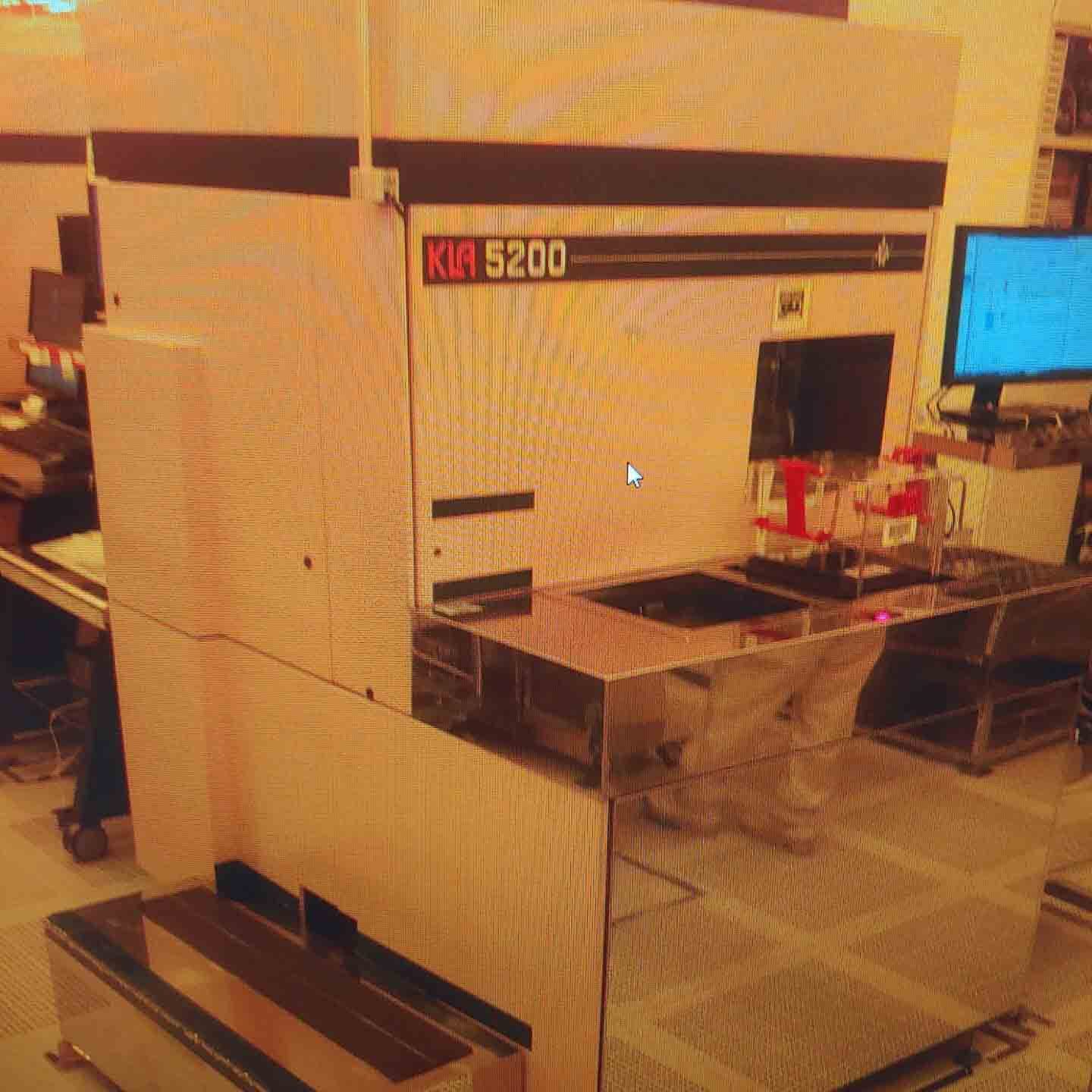
Used KLA / TENCOR 5200 #293603874 for sale
It looks like this item has already been sold. Check similar products below or contact us and our experienced team will find it for you.
Tap to zoom


Sold
KLA / TENCOR 5200 Automated Wafer Metrology and Test Equipment is a fully automated metrology and test system designed to accelerate the development and manufacturing of semiconductor devices. It is ideal for integrated circuit (IC) packaging, IC fabrication and assembly, and Die-to-Wafer (DTW) testing. The unit offers high throughput, high-accuracy, and reliable test and inspection capabilities for wafer-level tests, such as dielectric layer thickness measurements, wafer reflectivity measurements, surface roughness measurements, optical inspections, and yield enhancement. The machine also supports the evaluation of a variety of materials, such as copper, copper-plated substances, dielectrics and glasses. KLA 5200 is a modular test and metrology tool, comprised of a number of subsystems. These subsystems are: - Wafer Load Port: The Wafer Load Port is the entry point for loading and unloading wafers. It has pneumatic wafer transfer and handling robots, as well as an aerodynamically balanced vision asset. - Wafer Changer Ports: Wafer Changer Ports are used to move and store wafers between the various subsystems. - Bias Station: The Bias Station is a high-speed, high-accuracy biasing and testing station. It is designed to perform a variety of wafer-level tests and measurements for production yield enhancement. - Alignment Station: The Alignment Station is used to align and secure the wafers before testing and metrology. The station is also used to secure and orient the wafers prior to the test and metrology processes. - Metrology Station: The Metrology Station is the main testing and metrology subsystem. It is designed to provide accurate, repeatable and reliable wafer-level tests and measurements. - CCD Camera: The CCD Camera is used for high-performance imaging and inspection of wafers. It is ideal for defect recognition and classification, as well as fine wafer pattern analysis. - Wafer Transport: The Wafer Transport model is used to move the wafers between the various subsystems. It is capable of carrying up to 120 wafers at a time. In addition to the above subsystems, TENCOR 5200 also includes a comprehensive software suite for automated control and data collection. The software provides a user-friendly interface for wafer inspection, monitoring, and managing all aspects of the equipment, including system setup, wafer loading, process parameter configuration, and test results. Overall, 5200 Wafer Test and Metrology Unit offers a comprehensive, high-throughput, high-accuracy testing and metrology solution for the development and manufacturing of semiconductor devices. It enables fast and reliable dielectric layer thickness measurements, wafer reflectivity measurements, surface roughness measurements, optical inspections, and yield enhancement.
There are no reviews yet