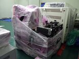
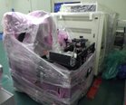
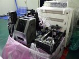
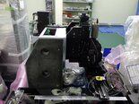
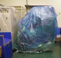
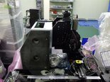
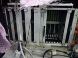
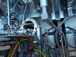
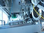
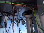
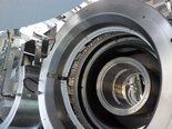
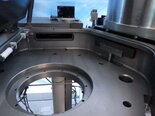
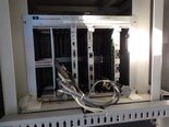
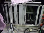
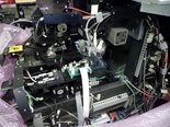
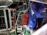
Used KLA / TENCOR 5200 #293645816 for sale
URL successfully copied!
Tap to zoom
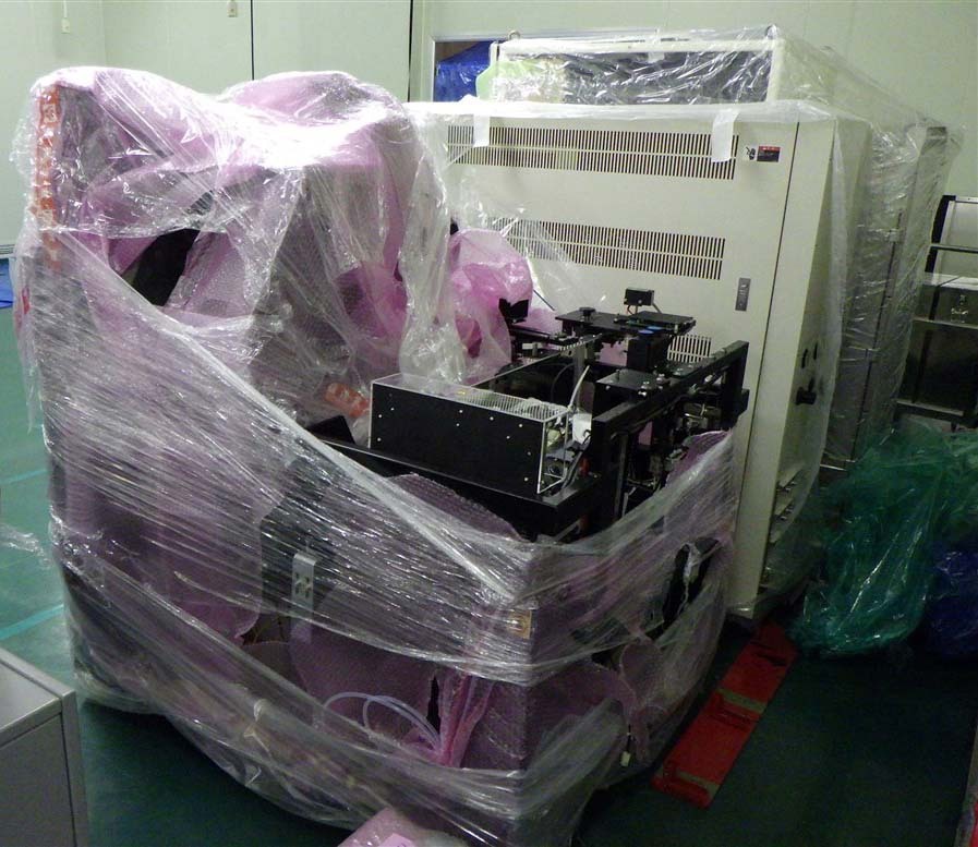

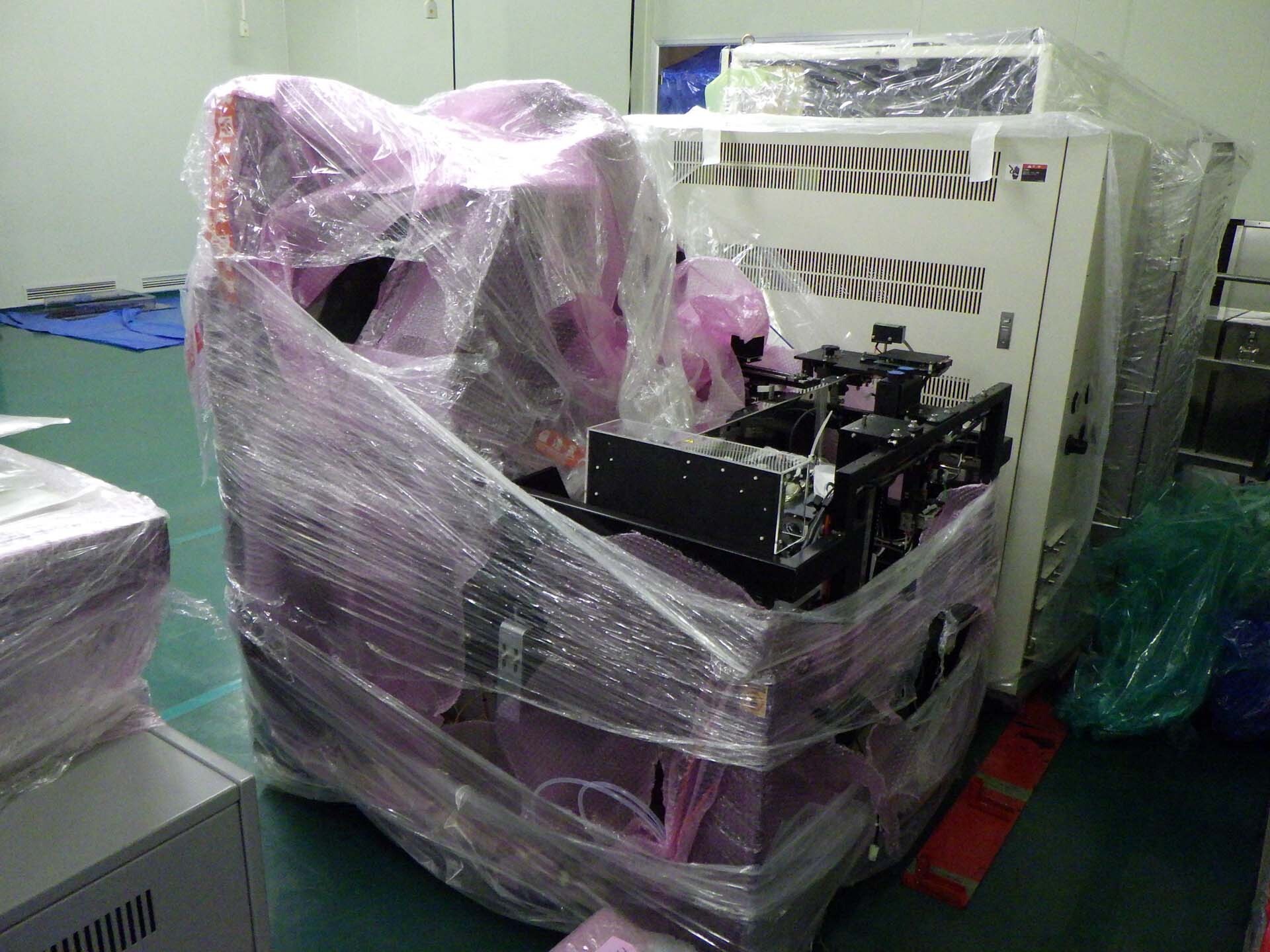


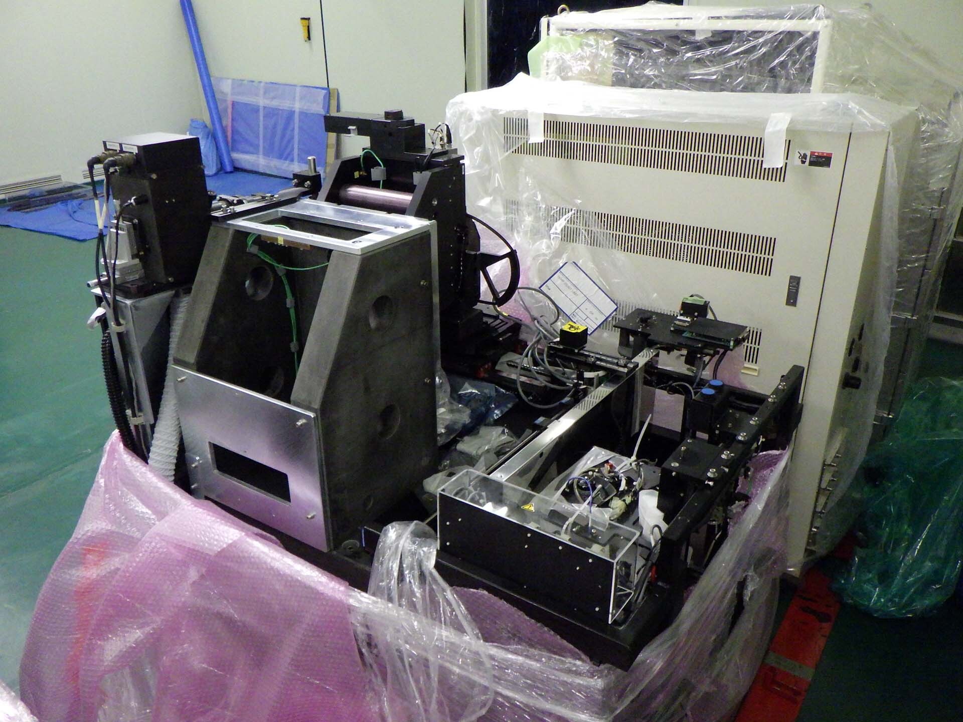

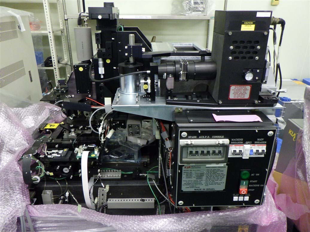


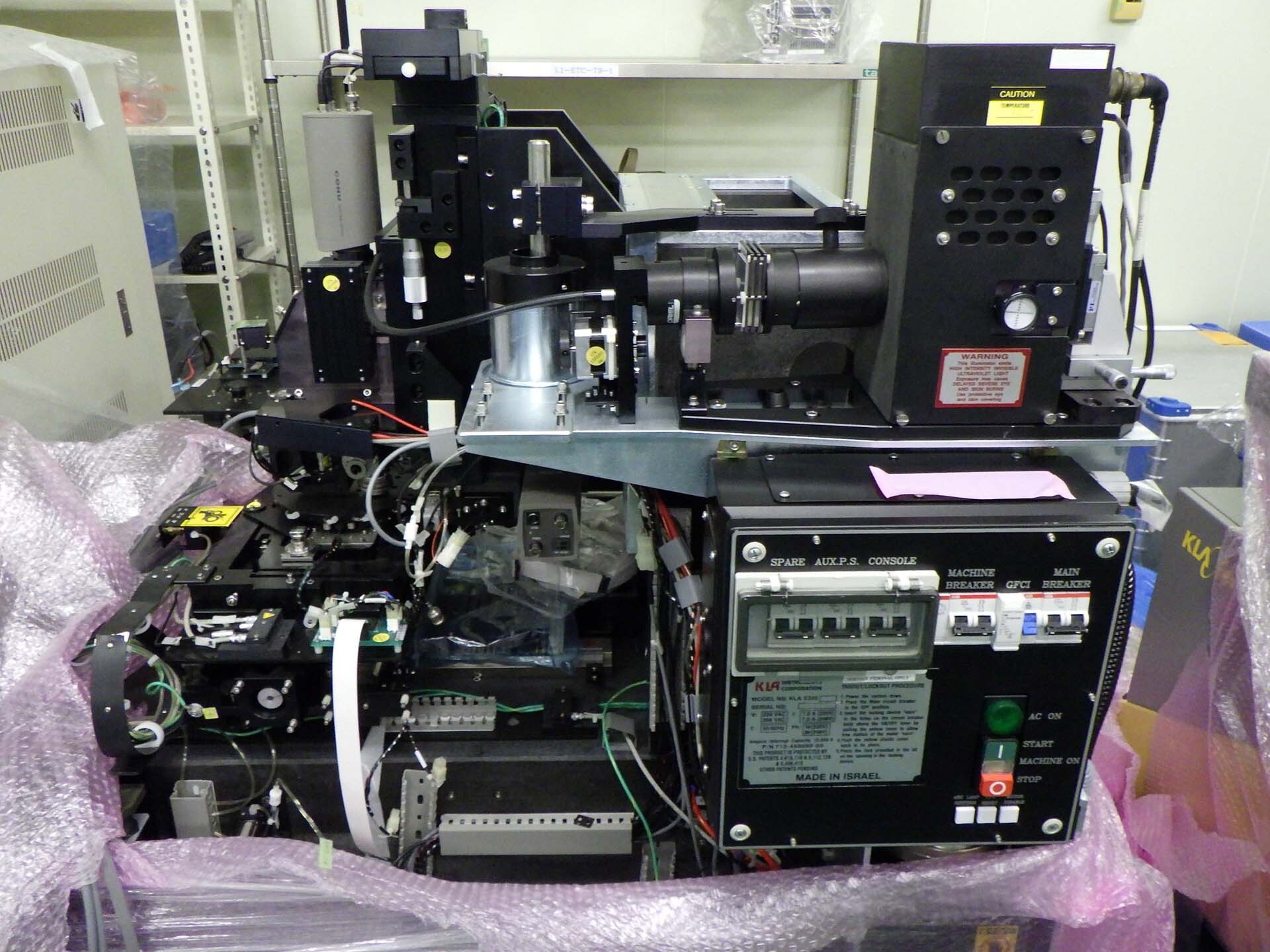


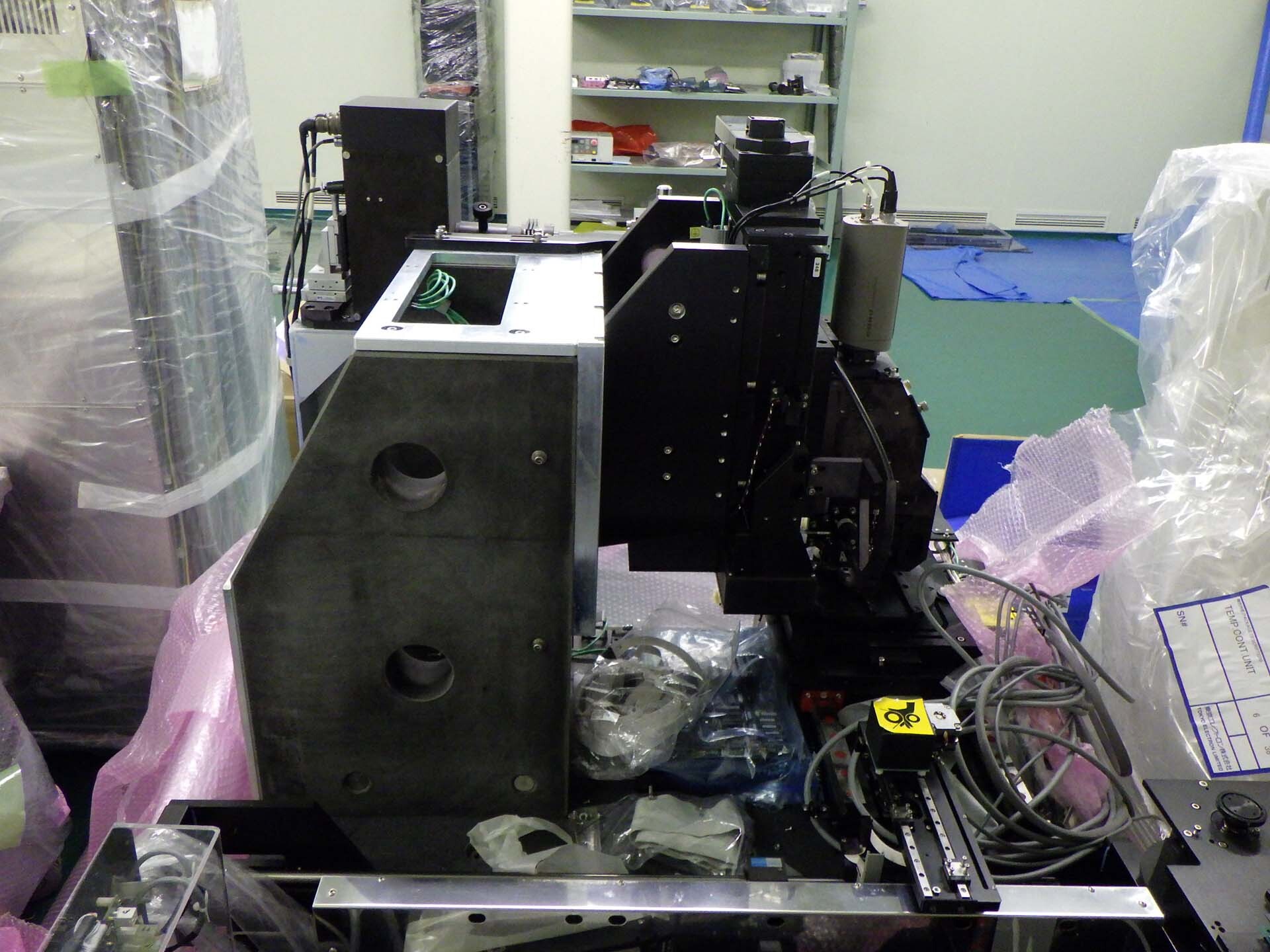

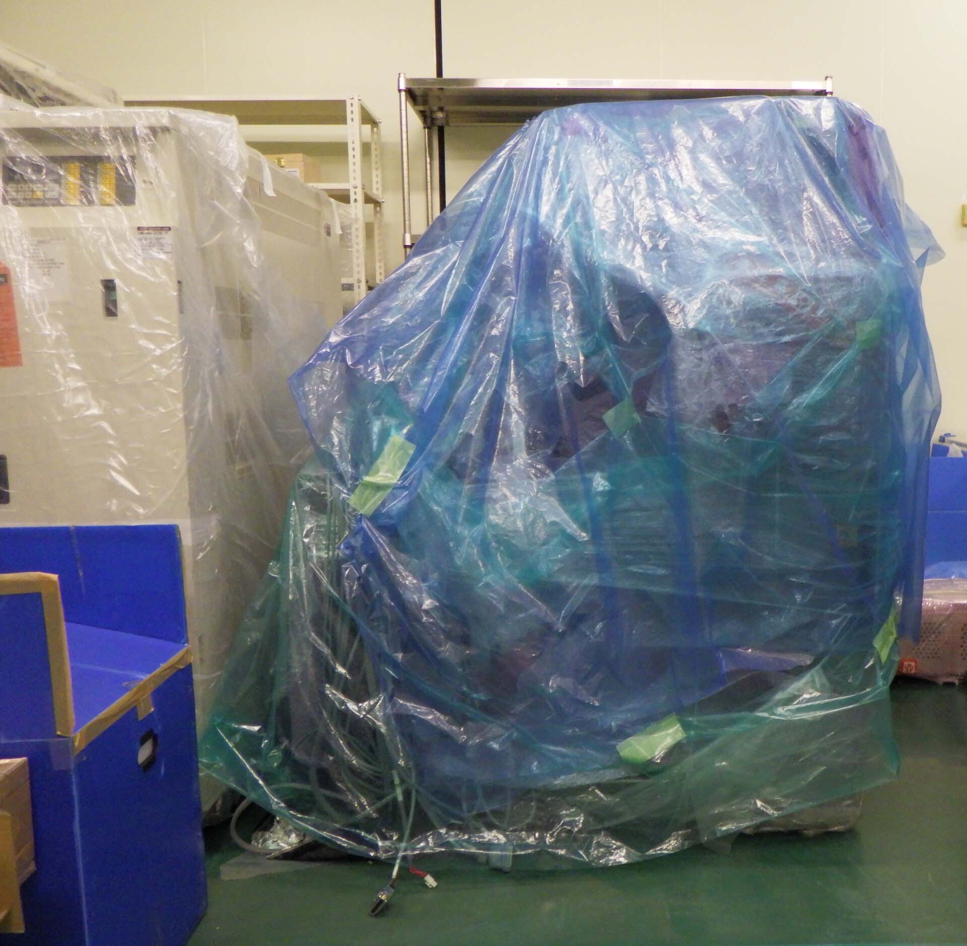

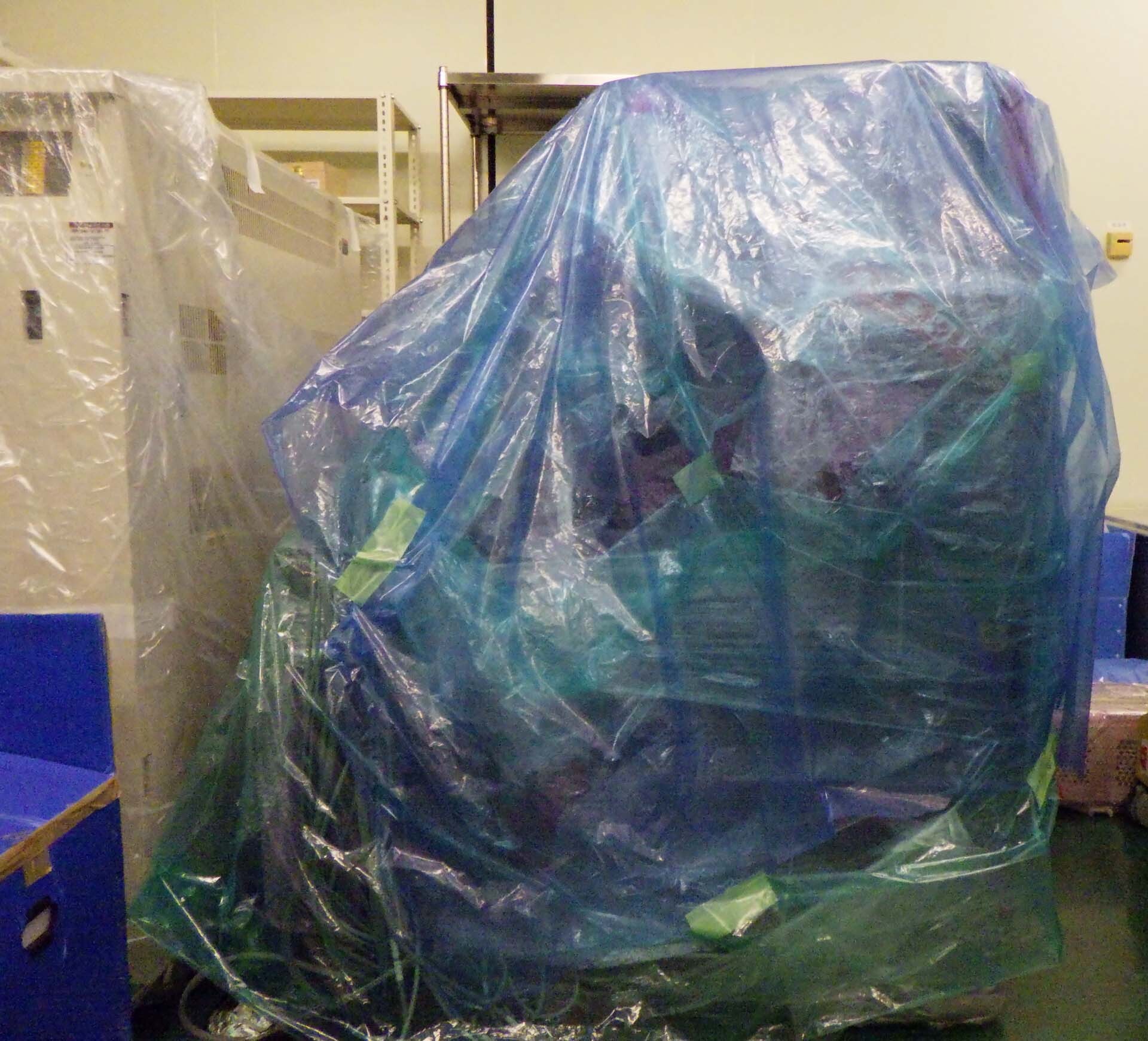

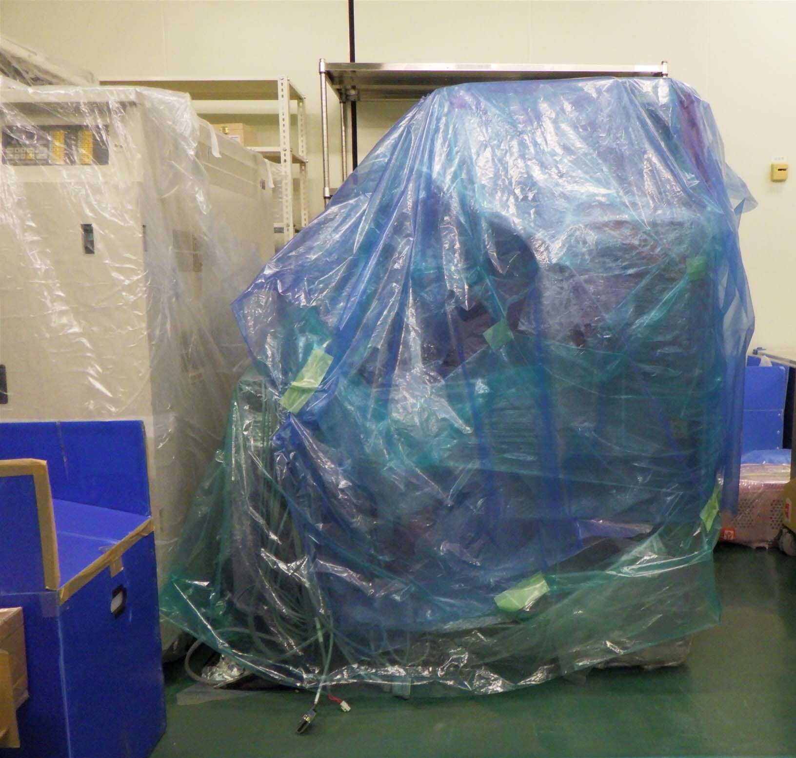

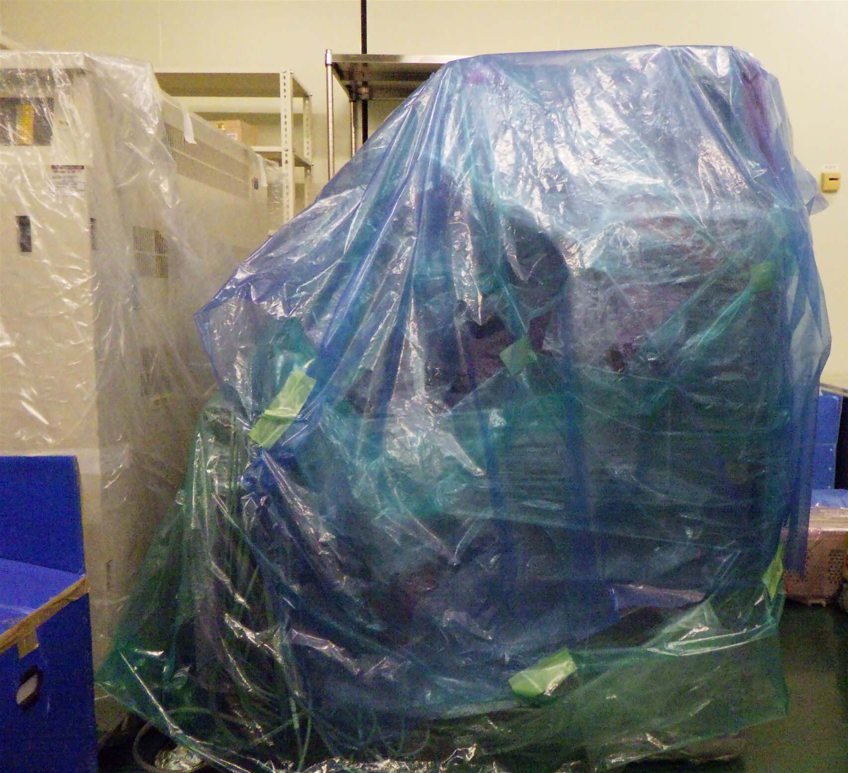


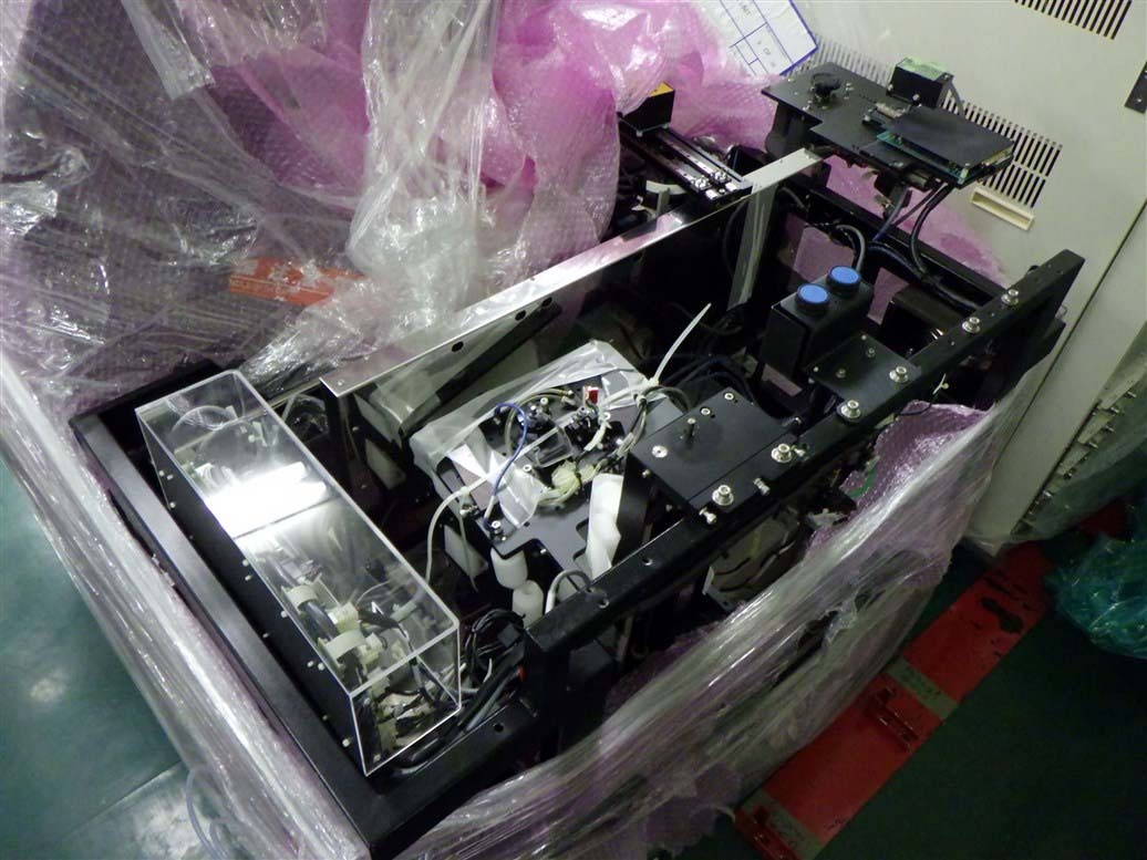

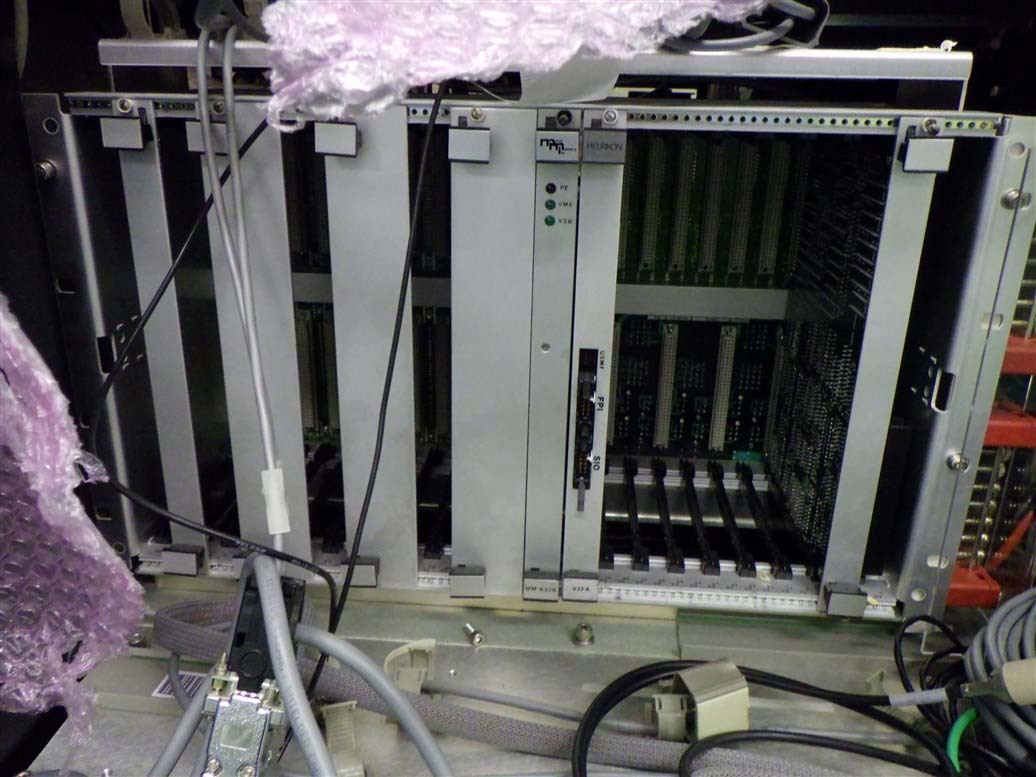


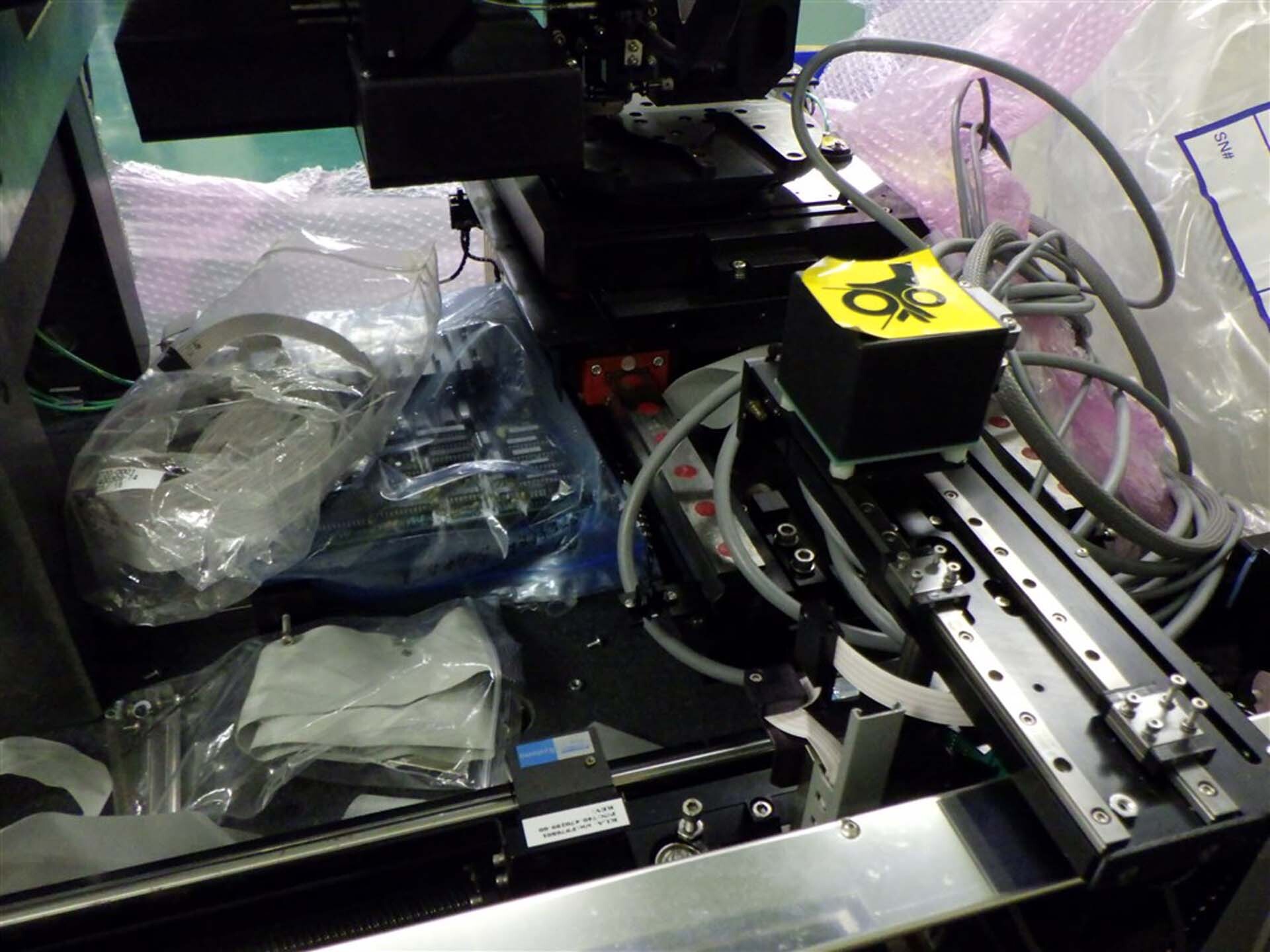

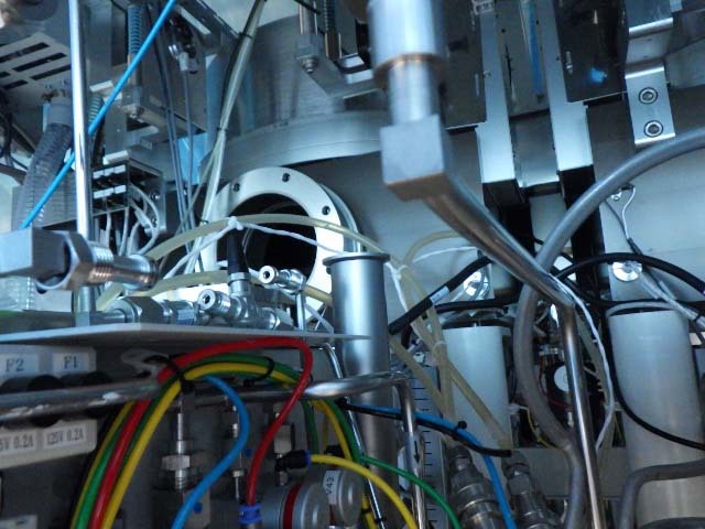

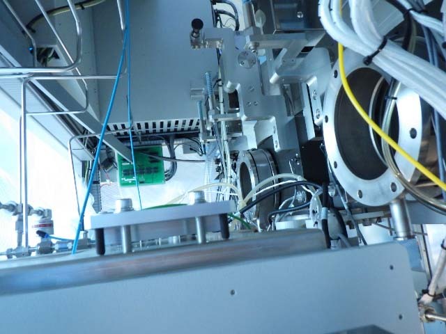

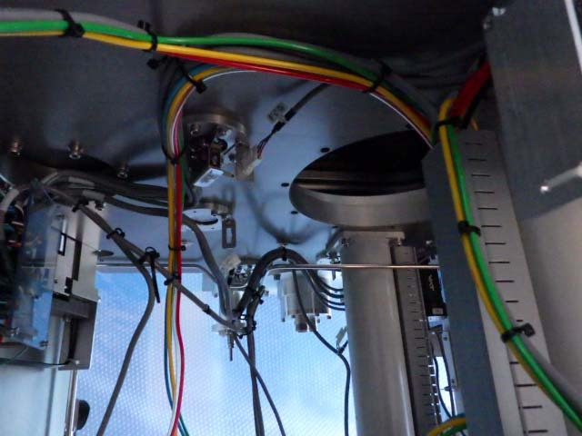


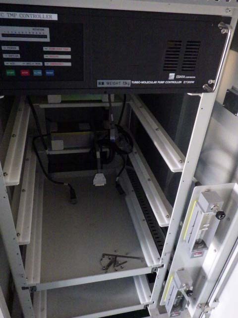


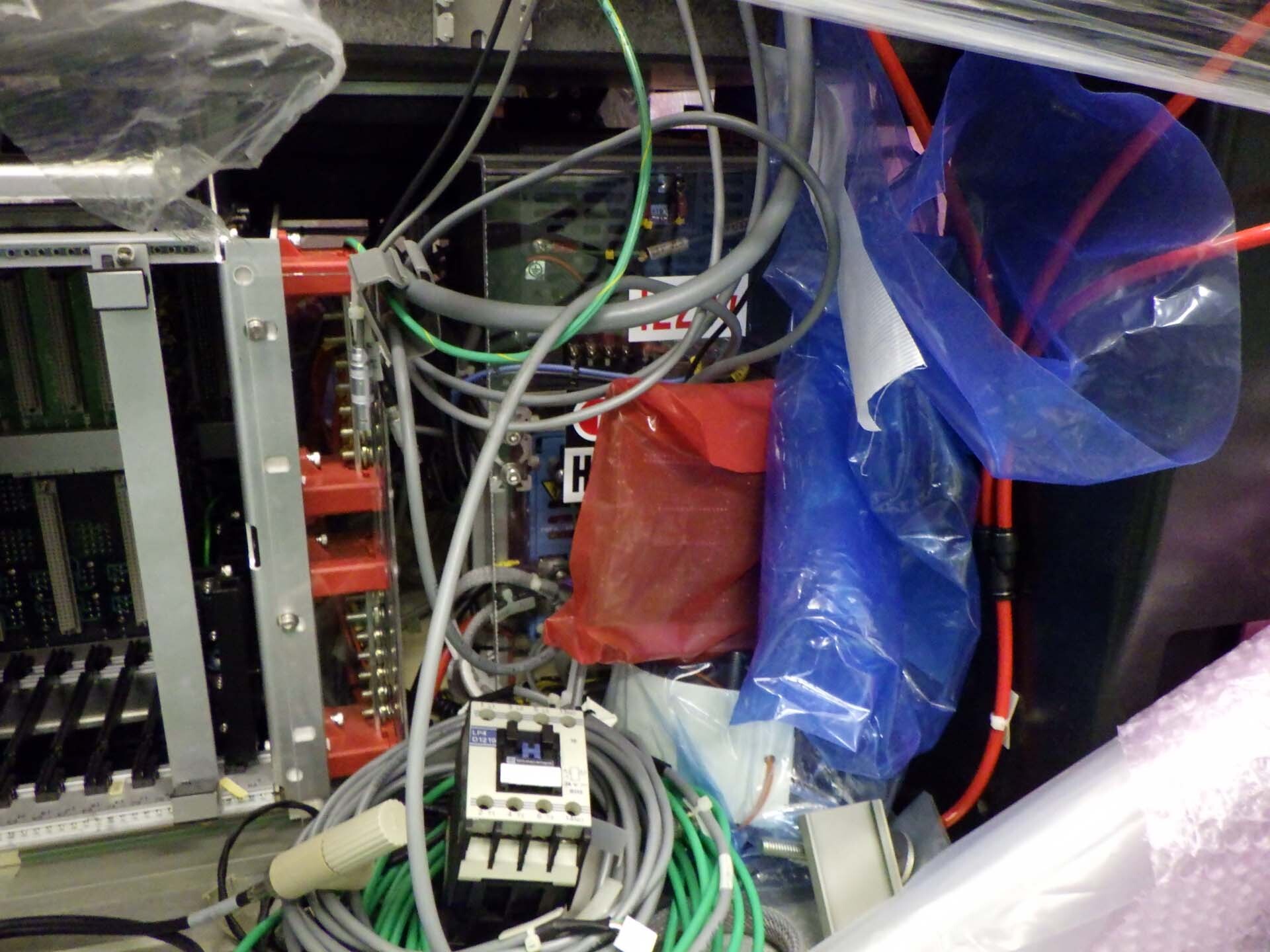


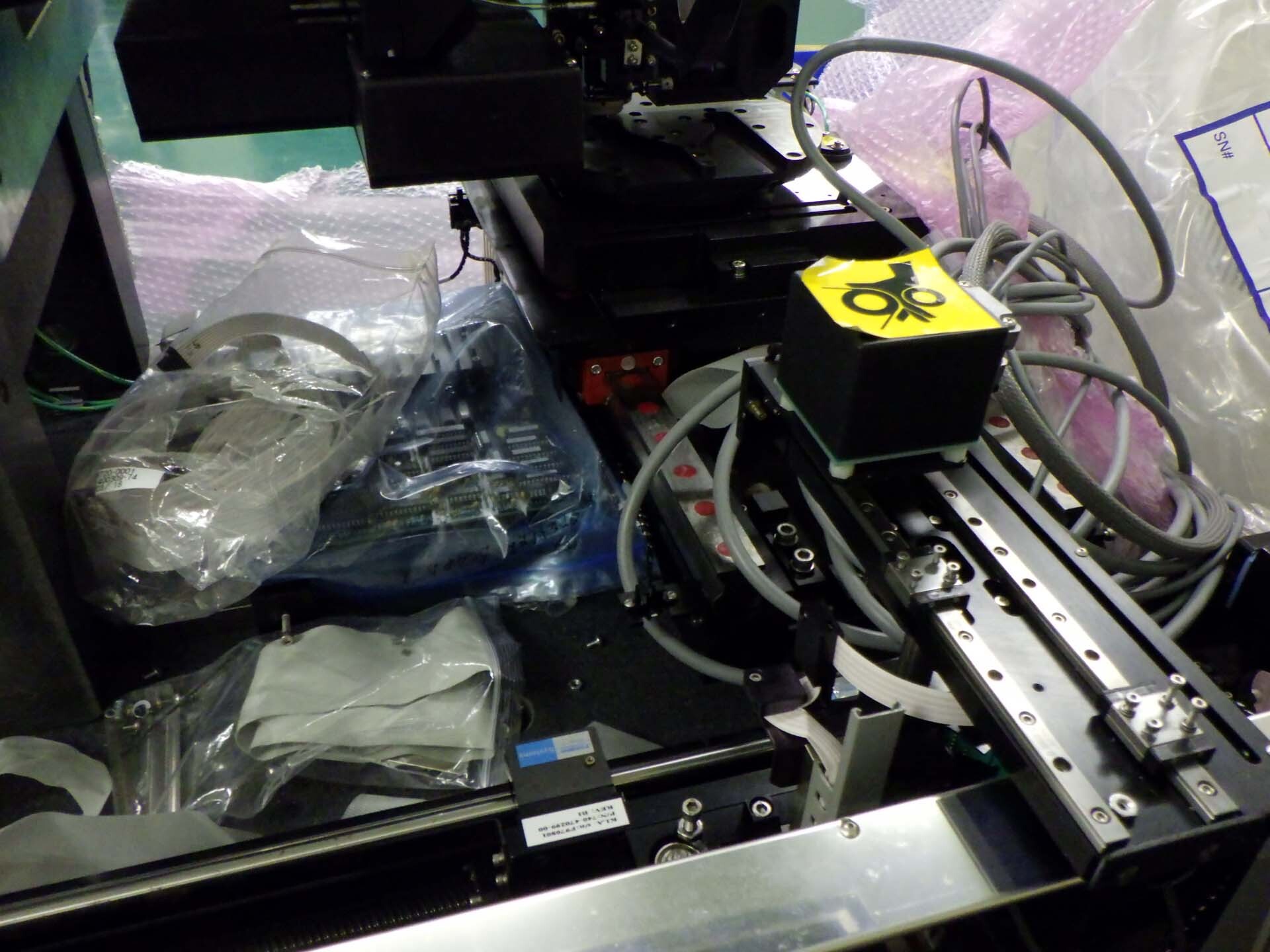


KLA / TENCOR 5200 is an advanced wafer testing and metrology system that enables semiconductor manufacturers to thoroughly evaluate the performance and yield of their wafers. KLA 5200 has capabilities for defect detection, surface topography imaging, quantitative film thickness measurement, critical dimension measurement, stress characterization, and overlay inspection. With these features, TENCOR 5200 is able to detect and analyze defects, evaluate uniformity and performance of material deposition, measure geometry and yield of patterned layers, analyze stresses, and check for overlay errors. 5200's defect detection tools inspect the wafer with an array of advanced sensors. Through SEM imaging, reflected electrons are captured which are then analyzed using KLA / TENCOR 5200's image processing algorithms. This allows the system to identify and distinguish various types of defects within the wafer. For surface topography imaging, KLA 5200 utilizes laser sources and critical dimension measurements. By analyzing the topographical characteristics of the surface, TENCOR 5200 is able to measure and calculate the height, or step height, of a surface and its lateral dimensions including the critical dimensions. This can include mapping a single material or differences and features between two material layers. 5200's film thickness measurement uses calibrated sources to non-destructively measure the thickness of thin films. This tool ensures uniformity and desired thickness of layers by analyzing the film's profile and then collecting measurements from 0-1000 nanometres. KLA / TENCOR 5200 is also able to detect nd characterize stress at the wafer level. Viscoelastic models are utilized to measure the change in stress over time, as well as parameters such as modulus, damping, and Poisson's ratio. Stresses may be caused by things such as thermal mismatch, material deformation, and lithography errors, among others. Finally, KLA 5200 is equipped with overlay inspection capabilities. By precise accuracy, precise measurements of the relative positions divided by two layers on a wafer, and the rotation between them, TENCOR 5200 can detect overlapping, non-overlapping and rotated patterns. Overall, 5200 is an incredibly precise and capable wafer testing and metrology system, with a wide range of capabilities for defect detection, surface topography imaging, film thickness measurement, stress characterization, and overlay inspection. Its advanced tools can be utilized to measure geometry and yield, detect defects, and analyze film characteristics, ensuring that successful, high-performing semiconductor devices are created.
There are no reviews yet

