Used KLA / TENCOR 5200 #293808796 for sale
URL successfully copied!
Tap to zoom
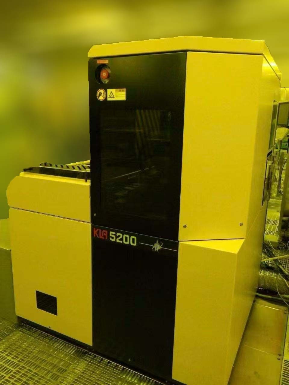

KLA / TENCOR 5200 is a high-speed wafer testing and metrology equipment that provides precise measurements of semiconductor topographies, surface structures, and chemical properties. The system is designed to accommodate up to 200mm semiconductor wafers, and its advanced technology enables it to measure features as small as 0.3 microns with ultra-high accuracy. KLA 5200 utilizes a variety of advanced, precision optical sensors and software algorithms that enable detailed characterizations of each wafer step. The unit may be outfitted with several high-performance optical sensors that are optimized for different measurements, such as laser interferometery for surface flatness, white-light interferometry for precise thickness measurements, and monochromatic optical profilometry for high-resolution imaging. The machine's capabilities are further enriched with the addition of an automatic probe station, which allows users to rapidly load and unload wafers at high speeds. Additionally, the tool enables precise analysis of wafer defects, and accurate analysis of real-time data including minimum topography and thickness measurements, along with the ability to compare features between wafers. TENCOR 5200 employs full-wafer microscopy imaging to capture high-resolution images of microstructural features, as well as single-die imaging to provide a comprehensive view of the entire wafer. Through the use of a patented Wafer Pattern Summarization (WPS) technique, the asset generates a 3-dimensional representation of the entire wafer's topography, which allows for precise analysis of thin and thick film surfaces, multiple process layers, and other fine-scale features. 5200 also provides a unique combination of automated and manual measurements to facilitate the optimization of etch and CMP processes. The model has the capability to measure cross sections, as well as depths of V-depressed and pin holes. In addition, the automated machine vision feature allows for automated binning of wafers and pattern matching, even when using low-power illumination. Overall, KLA/Sequent KLA / TENCOR 5200 is a powerful and cost-effective solution for the precise testing and metrology of 200mm semiconductor wafers. It combines advanced optical sensors and specialized algorithms to deliver highly accurate measurement measurements, as well as detailed analysis of defects, topography, thickness, cross sectional image and pattern matching. With a suite of advanced features and capabilities, KLA 5200 can provide the in-depth analysis required to ensure the integrity of today's semiconductor devices.
There are no reviews yet