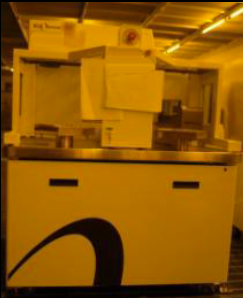
Used KLA / TENCOR 5300 #120993 for sale
It looks like this item has already been sold. Check similar products below or contact us and our experienced team will find it for you.
Tap to zoom


Sold
ID: 120993
Wafer Size: 8"
Vintage: 2001
Overlay measurement system, 8"
Process: PEP
Control console:
Console PC
Monitor
Keyboard and trackball
Video printer
Sub storage device (CD/floppy/tape)
Power and signal cables
Handler:
Robot
Power and signal cables
Inspection station:
Main body stage
X-Y chuck stage
Optics
Power and signal cables
Includes:
Lexmark printer
Backup floppies (1 set)
Spanner
208 V, 1 phase, 50/60 Hz, 12.5 A
2001 vintage.
KLA / TENCOR 5300 is a state-of-the-art wafer testing and metrology equipment. It is designed for advanced defect inspection and process control. KLA 5300 achieves high sensitivity with three separate technologies: Automated Optical Inspection (AOI), Automatic Defect Recognition (ADR), and Sub-Pixel Imaging System (SIM). The AOI uses a charge-coupled device (CCD) camera to capture high-resolution images of the wafer. With on-board image processing, the unit identifies and identifies defects in real-time. The machine is capable of detecting sub-micron defects and can identify a range of both electrical and optical characteristics, including shorts, opens, defects, solder bridge, and alignment issues. The ADR is tailored to detect specific types of defects. It performs a deep analysis of the image, searching for patterns and correlation between areas of the wafer. This allows it to detect even the smallest of defects. The ADR also provides traceability and traceability analysis, allowing for greater process control and in-depth yield analysis. The SIM technology is at the core of TENCOR 5300, allowing it to detect nanometer-level structure defects. By creating high-resolution images of the wafer, it allows the tool to detect a wide variety of defects, including line width mismatches, missing structures, and displacement shifts. It can also analyze the results of the AOI and the ADR and provide a detailed assessment of the wafer structure. Overall, 5300 is a powerful tool for wafer testing and metrology. It provides high sensitivity, advanced defect detection, and more comprehensive analysis for process control. With its robust features, it can help improve yield and production quality and reduce time to market.
There are no reviews yet