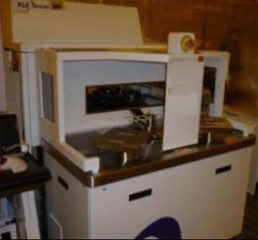
Used KLA / TENCOR 5300 #9193654 for sale
It looks like this item has already been sold. Check similar products below or contact us and our experienced team will find it for you.
Tap to zoom


Sold
ID: 9193654
Wafer Size: 8"
Vintage: 2001
Overlay measurement system, 8"
Process: PEP
Control console:
PC Console
Monitor
Keyboard & mouse (Track ball)
Video printer
Sub storage device: (CD / Floppy / Tape)
Power / Signal cables
Handler:
Robot
Power / Signal cables
Inspection station:
Mainbody stage
Chuck stage: X / Y
Optic
Power / Signal cables
Accessories included:
Line conditioner
Handler
DSW
Manuals
Power supply: 208 V, 12.5 A, Single phase, 50/60 Hz
2001 vintage.
KLA / TENCOR 5300 is a state-of-the-art wafer testing and metrology equipment designed for the semiconductor industry. It combines advanced wafer testing, images, and metrology capabilities in a single, integrated system. It is a high-speed, precise and accurate tool for measuring, analyzing, and assessing a wide range of wafers and components. KLA 5300 unit incorporates advanced image analysis technology to automatically analyze highly detailed images of wafers and allows for higher accuracy measurements on wider ranges of grinding and polishing materials. It also provides precisely measured test results from a single test point, which can be examined quickly and efficiently. The machine is capable of analyzing highly reflective surfaces such as high-k dielectric films, high- performances interconnects, and advanced designs. It also provides high-resolution measurements of nano-scale features without the need for specialized tools or specialized preparation. TENCOR 5300 has a high-precision, ultra-fast scanning tool, which allows for rapid analysis of single points or large arrays of points with no artifacts present. Additionally, its automated image pre-processing feature automatically optimizes images for contrast and shadow effects to provide the most accurate image analysis available. The asset also features a Macro Processor Suite, which allows for rapid image processing and analysis of complex structures. It can also examine the environmental conditions and material properties of wafers and components with its ABM Application Suite, which provides personalized metrology of different materials and surface defects, and quick, automatic calibration and feature recognition for pattern matching. 5300 is a simple but powerful model that enables automated and precise wafer testing, metrology, and imaging for the semiconductor industry. It can accurately analyze complex structures and provide fast and accurate results, allowing for more efficient manufacturing processes and higher levels of quality control.
There are no reviews yet