Used KLA / TENCOR 6200 Surfscan #293776296 for sale
URL successfully copied!
Tap to zoom
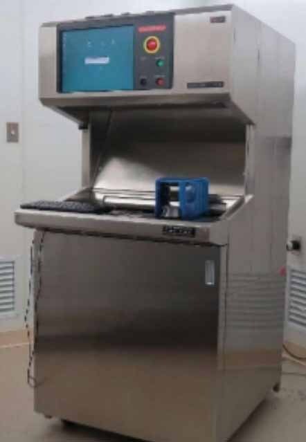

ID: 293776296
Inspection system
Solid state laser
Control box
Wafer paddle
Indexer
Shuttle drive
Motor
Belt
Bearing
Lead screw nut assembly
Solid state hard drive
Load arm
Lead screw
Cassette elevator
Re-anodize plate
Cover
Frame
PC
Keypad
Mouse
LCD Monitor
USB 2.0
Power supply.
KLA / TENCOR SFS 6200 is a wafer testing and metrology equipment that is used by semiconductor manufacturers to measure selected parameters of integrated circuits on a silicon wafer. The system combines a highly-accurate wafer testing capability with a focused ion beam (FIB) unit for high-resolution surface imaging and an electron beam for sample preparation and analysis. The machine includes an advanced pattern recognition environment for correlating die-level data to features on the wafer surface. For testing, KLA SFS 6200 employs two methods: electrical and optical. Electrical testing is the process of offering electrical stimuli to the device, then measuring the responses and use them to identify defects. Optical testing uses a scanning electron microscope to image the wafer surface. By comparing measurements across wafers, engineers are able to detect differences in parameters such as edge profile, overlay alignment, critical dimension linearity and yield. Furthermore, the tool is able to identify defects and deviations in these measurements and alert the user. The FIB section of TENCOR SFS6200 contains three chambers, allowing the user to perform volume scope, surface imaging and site-specific sample preparation. The asset is equipped with a high-vacuum column, a high accuracy and dynamic level control, and high resolution imaging to ensure that the images produced are of the highest quality possible. The FIB chamber also contains a geometry and stress module, which is used to measure the local thermal expansion coefficient and surface layering of the sample. The electron beam section of SFS 6200 allows for sample preparation through sputter coating and provides high resolution imaging. The model's electron beam is able to penetrate deeper into the material than the FIB and allows for the user to detect sub-surface defects on the sample. This enables a deeper understanding of the device or process under investigation. In addition to wafer testing and metrology, KLA / TENCOR SFS6200 can also be used for defect review, failure analysis and product engineering. The equipment's high-throughput and robust design makes it an ideal option for semiconductor manufacturers that need accurate testing and results in a timely manner.
There are no reviews yet