Used KLA / TENCOR 6200 Surfscan #293829830 for sale
URL successfully copied!
Tap to zoom
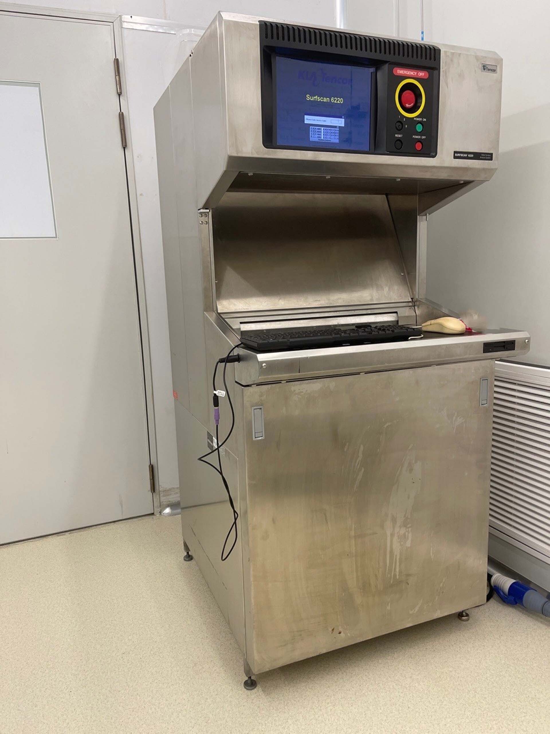

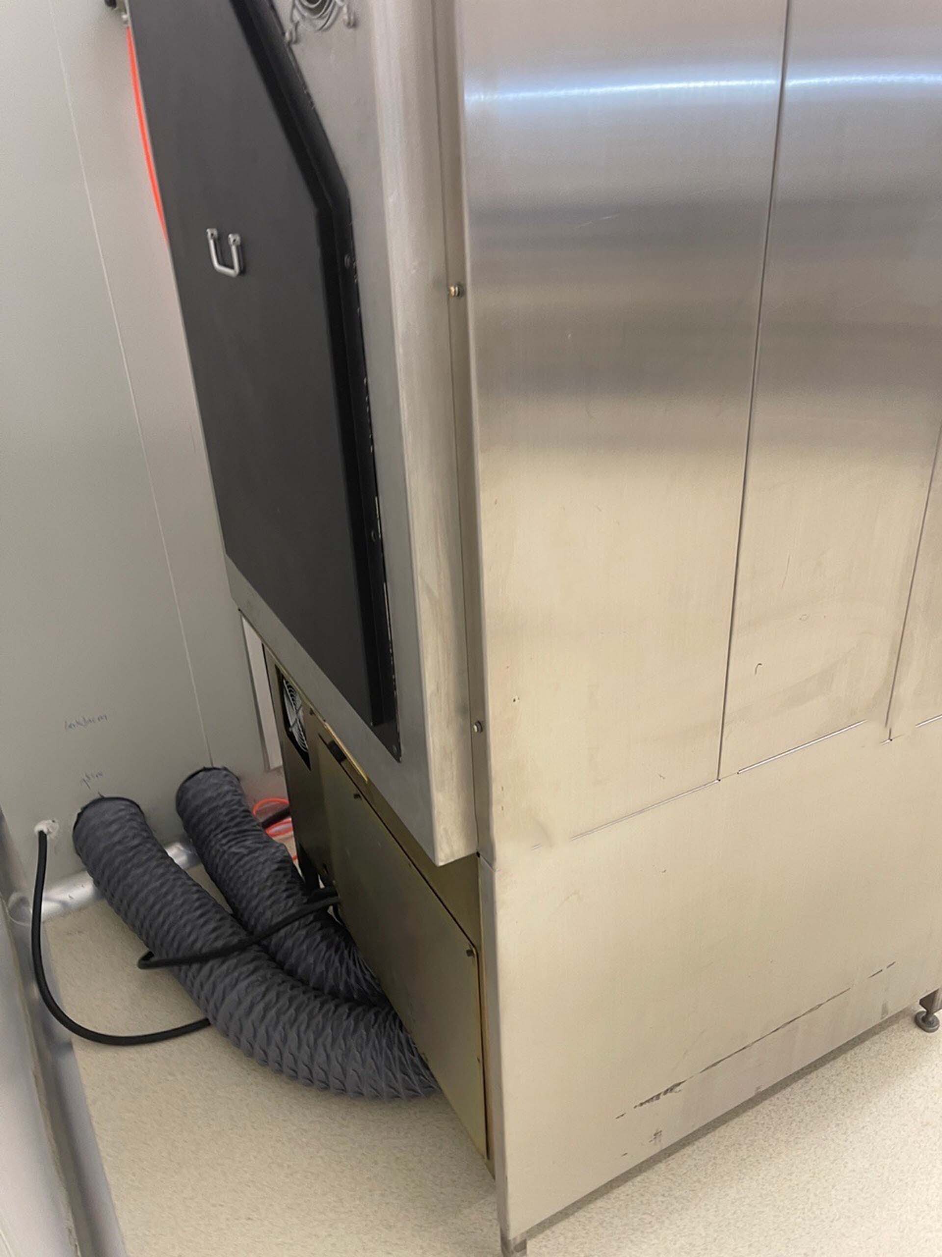
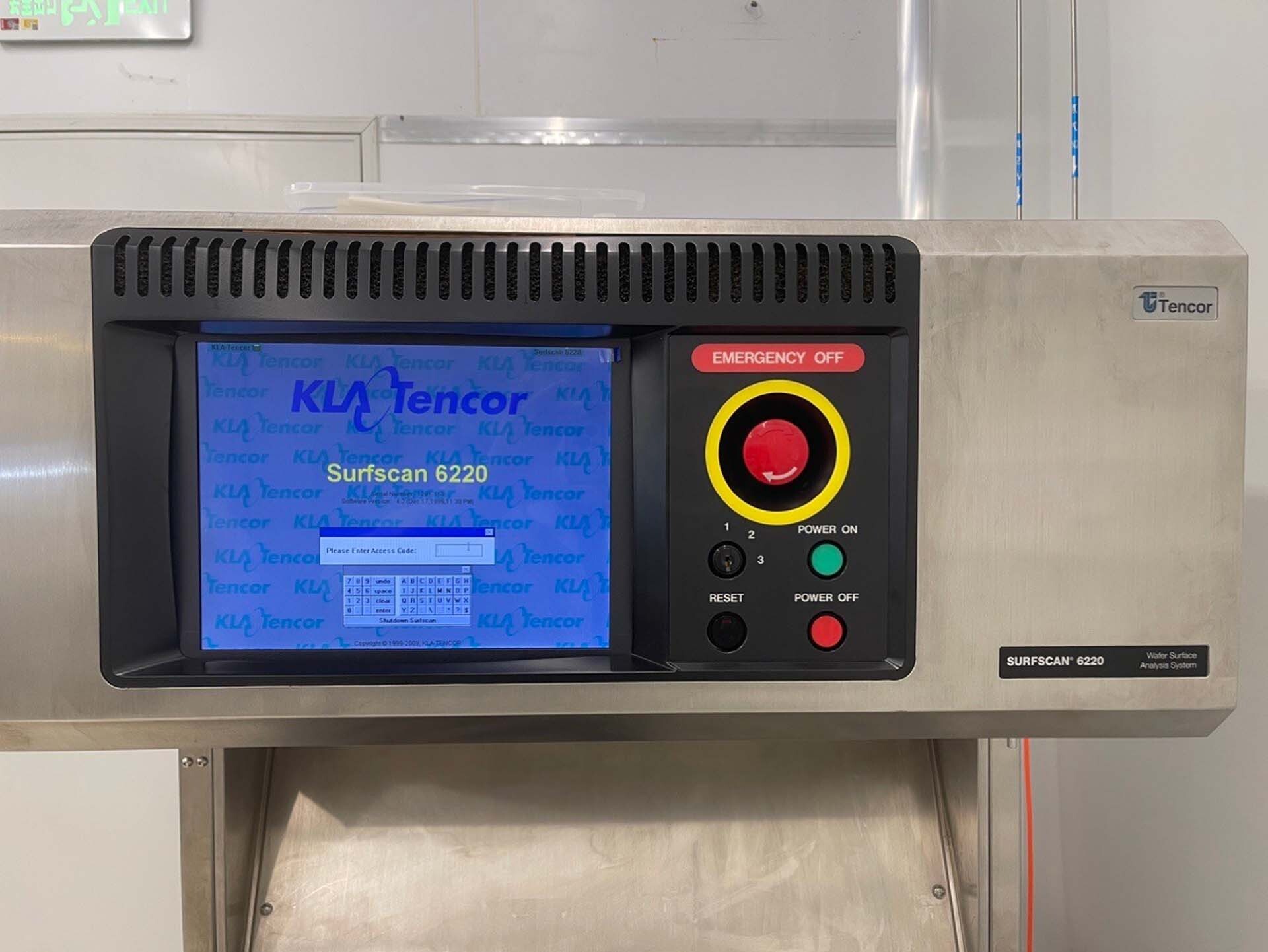
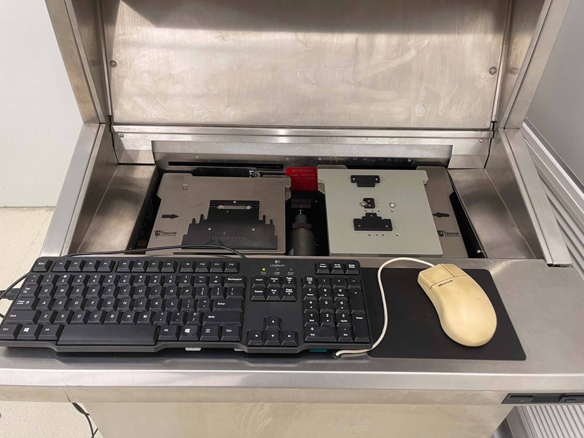
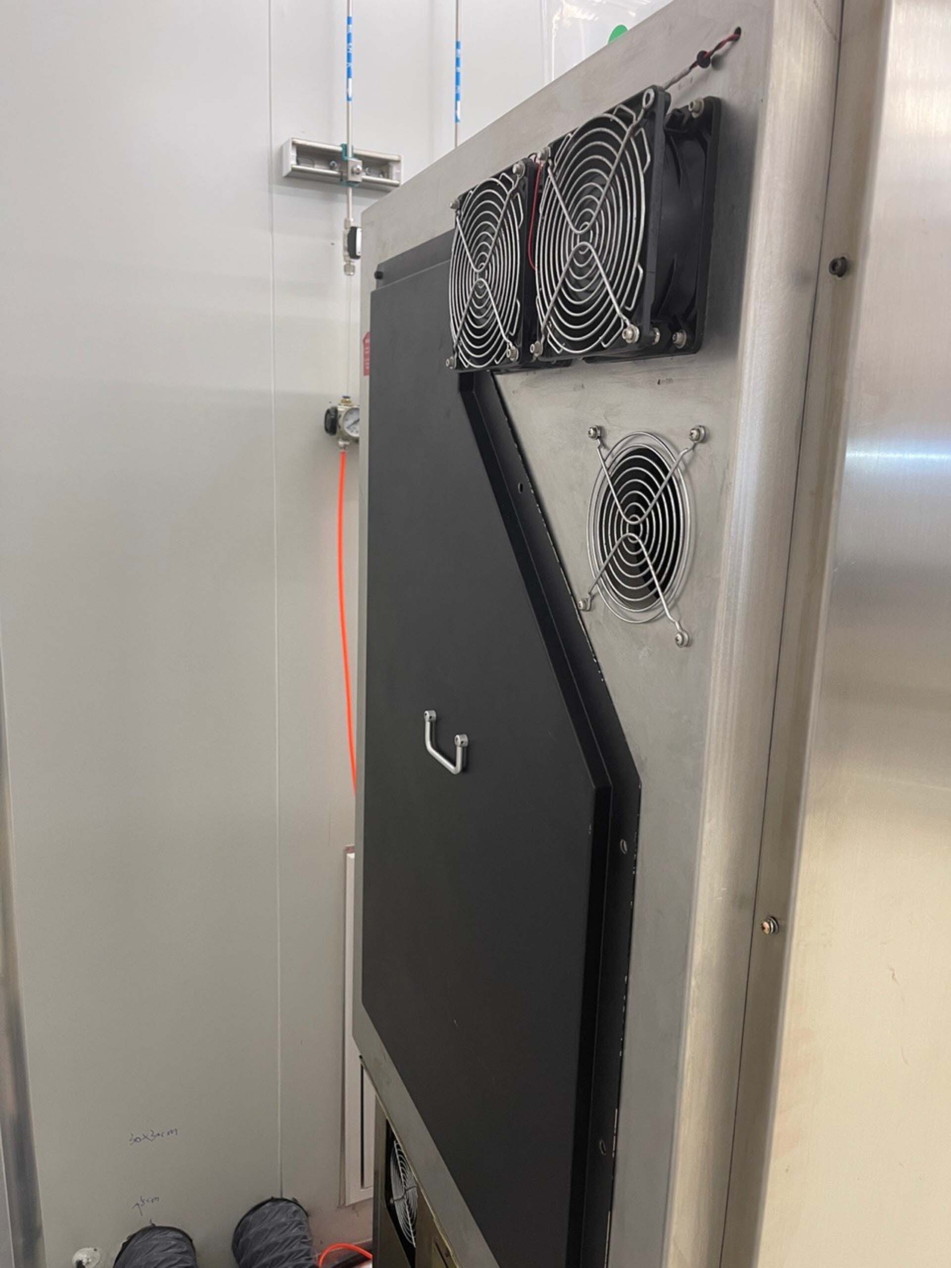
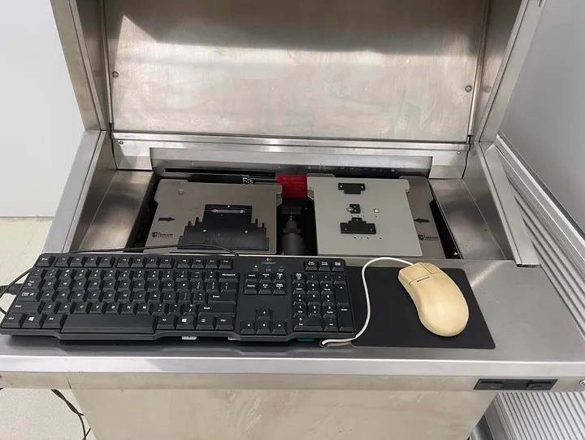
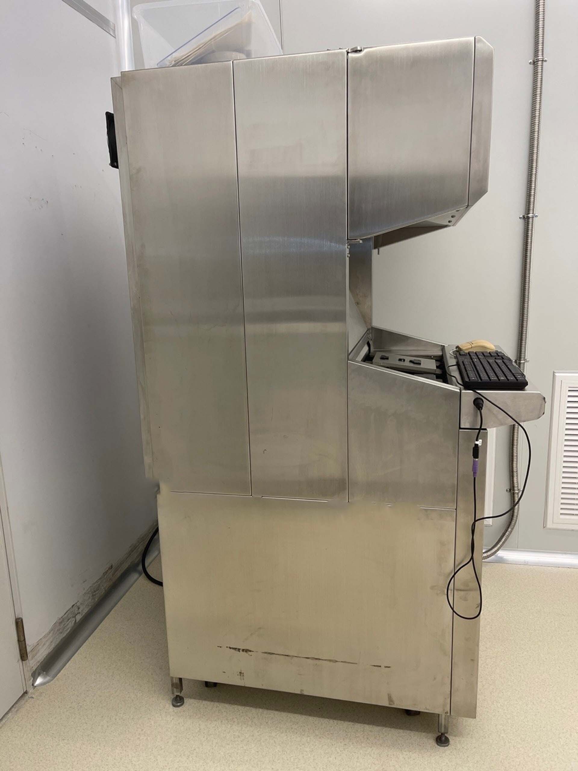
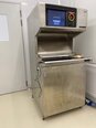
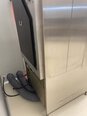
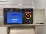
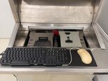
KLA / TENCOR SFS 6200 is a wafer testing and metrology equipment used in the semiconductor industry to analyze the surface characteristics of wafers at the nanometer scale. KLA SFS 6200 provides fast, accurate, and reliable wafer metrology capabilities for a wide range of semiconductor fabrication processes, including lithography, deposition, etching, and defect inspection. The system is designed for inspection and analysis of various materials, and features a robust, multichannel design to optimize data collection speed and accuracy. The unit is capable of capturing images up to 10,000 µm in size and with resolution down to 10 nm. It features an ultra-sensitive AFM cantilever that can measure 3D topography, 2D profile, 2D defect, and 3D defect detection. Additionally, TENCOR SFS6200 has multiple frequency channels, each capable of precisely measuring the amplitude and phase of the cantilever peaks and valleys. KLA / TENCOR SFS6200 also supports a suite of corrosion or scratch testing to evaluate the performance of surfaces. This feature enables micro-scale surface evaluation and can be used for studying the effects of stress on specimen material or for process control and qualification. SFS 6200 is equipped with advanced algorithms and 3D localization capabilities to analyze surface characteristics, with the capacity to measure defect size, shape, and height. SFS6200 includes intuitive user interface software specifically created to simplify data collection and analysis operations. The simple UI combines powerful software, graphical analysis tools, and secure data sharing capabilities to ensure fast, reproducible measurements. The machine is also equipped with remote reporting, scheduling, and tracking features that allow users to monitor and control the analysis process. The tool includes AutoProbe software, a powerful signal analysis and characterization package that provides fully automated results. Users can configure signal traces and create 3D profiles of features. For complex features, directional signal analysis capabilities allow users to obtain spectroscopic information to optimize their process. In conclusion, KLA SFS6200 is an advanced wafer testing and metrology asset designed to speed up and improve performance in the semiconductor industry. The model offers reliable testing and metrology capabilities with a robust design, multiple frequency channels, corrosion or scratch testing, and automated signal analysis tools. Additionally, the intuitive user interface ensures easy data collection, analysis, and sharing.
There are no reviews yet