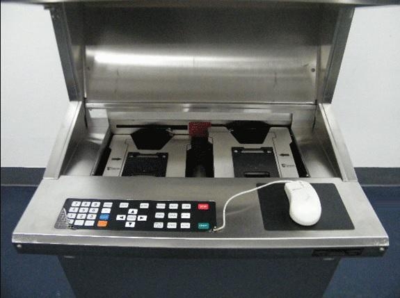
Used KLA / TENCOR 6220 Surfscan #9194019 for sale
URL successfully copied!
Tap to zoom


ID: 9194019
Automatic surface inspection system
Bare wafer surface defect inspection system
Left side: 4"/6" wafers
Right side: 2"/3" wafers
Thickness: SEMI Standard wafer thickness
Throughput: 100 wph (200 mm) at 0.12 mm
Illumination source: 30 mW Argon-Ion laser / 488 nm Wavelength
Operator interface: Mouse / Dedicated user keypad
Operations manual / Documentation
Material:
Any opaque
Polished surface (Scatters less than 5 percent of incident light)
Defect sensitivity:
Micrometer diameter: 0.09
PSL Sphere equivalent (>80 percent capture rate (0.112um @ 90%))
Repeatability:
Count repeatability: <0.5 percent at 1 standard deviation
Mean count: >500, 0.364 mm Diameter / Latex spheres
Accuracy:
Count accuracy better than 99 percent
VLSI Standards relative standard
Contamination (Per single pass):
<0.005 particles/cm²
>0.15 mm diameter
Cassette handling:
Single puck wafer handling from two cassettes
Sender / Receiver
Receiver.
KLA / TENCOR 6220 Surfscan is a wafer testing and metrology equipment that is designed to measure and inspect the physical characteristics of semiconductor devices. The system is designed to provide precise measurements of the profiles of features on silicon wafers and can detect defects within each wafer. It is capable of fully automated operation, scanning large numbers of wafers in quick succession with minimal intervention. The unit features a four-axis stage design with precision motors and feedback systems that scan wafers up to 300 mm in diameter at a speed of up to 500 mm/sec. The scan parameters can be adjusted to achieve the desired resolution, with the standard machine configurable for scans with a 50 μm resolution. The tool also features an optical asset with a high-speed camera and a broadband light source. This provides images of features on wafers with images being captured at 10,000 frames per second. The captured images are then analysed by software that can detect any defects present, which are then classified by size, shape, or other characteristics. The model can be used for process control, wafer mapping, and yield management. This allows for a better understanding of what is happening in a particular process and make corrections before any potential defects become significant. It also allows for faster wafer processing, increasing productivity as well as reducing costs. In addition to wafer inspection, KLA 6220 Surfscan equipment can also be used for other processes such as metrology, contact angle measurements, film thickness measurements, and determination of surface roughness. This allows for a detailed understanding of the characteristics of a particular material, giving engineers and scientists more information to work with. Overall, TENCOR 6220 Surfscan system is a powerful and versatile tool that can be used to quickly and efficiently inspect wafers for any defects, as well as analyse other characteristics of the material. Its combination of precision, speed, and software optimisation makes this an invaluable part of any semiconductor production process and a great asset for the industry.
There are no reviews yet