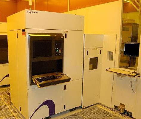
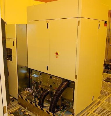
Used KLA / TENCOR AIT UV #9285827 for sale
URL successfully copied!
Tap to zoom
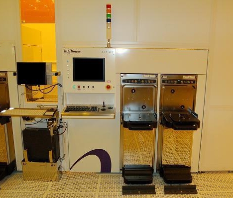



ID: 9285827
Wafer Size: 12"
Darkfield inspection system, 12"
SECS II / GEM Communication interface
High resolution chuck
Image grab feature
Multi channel collection optics system with independent programmable spatial filters and adaptive PMT modules
Image process computer
Blue laser: 448 nm
(2) FOUP Load ports
0.1 Micron detection
Un-patterned recipe capability.
KLA / TENCOR AIT UV is a next-generation metrology equipment. Its purpose is to measure the quality of wafers produced in a manufacturing environment. This is an essential process in the production of ICs, which require precise dimensional accuracy and process control. The system uses a combination of techniques to inspect the wafer in an ultra-violet environment. The technology employs advanced imaging, beam profiling and patterning capabilities to measure the wafer's surface to nanometer accuracy. This includes both optically and acoustically mapping the wafer. The imaging unit features a high-performance confocal microscope. This allows for more rigorous and accurate analysis than other systems. Its resolution and accuracy can measure surface features to the nanometer level. It is able to detect topography, surface finish, and uniformity. The beam profiling machine utilizes two-dimensional beam-shaped measurement capabilities. It enables high-speed and precise characterization of the wafer's surface. This helps to ensure that a proper relationship exists between the wafer and the substrate. Additionally, the patterning tool includes a nanometer-scale inspected feature transfer. This process is used to transfer a patterned layer from one substrate to another. This helps to improve the process parameters and maintain the necessary precision for manufacturing. This high-performance metrology asset provides excellent results and reliability. It is capable of measuring the critical features of the wafer, and helps to ensure that the wafers are consistent with the desired specifications. KLA AIT UV is the key to sustained wafer production quality and optimized process parameters. The model offers accuracy, precision, and repeatability needed to ensure that only acceptable wafers are used in the manufacturing process.
There are no reviews yet
