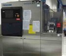
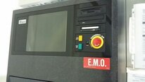
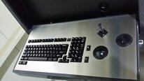
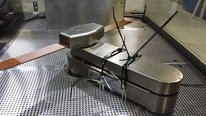
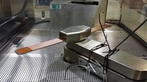
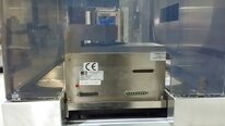
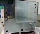
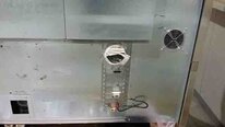
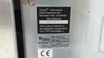
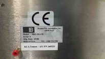
Used KLA / TENCOR AIT #293595750 for sale
URL successfully copied!
Tap to zoom


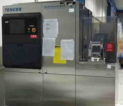


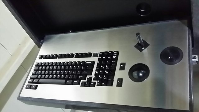

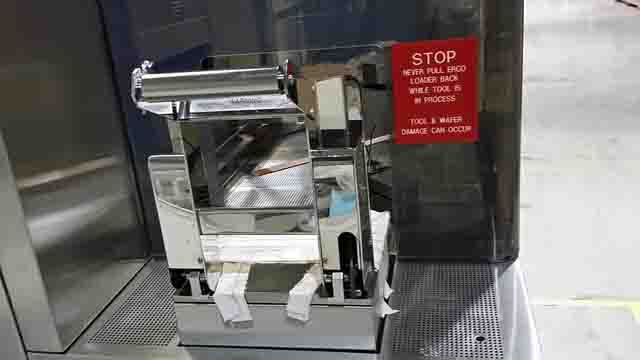


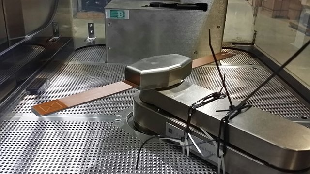

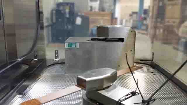


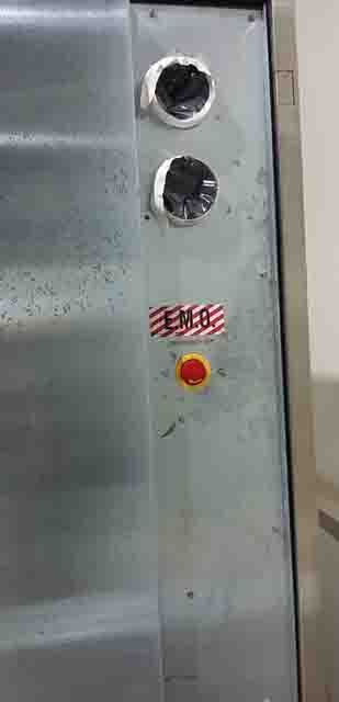

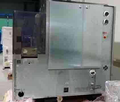

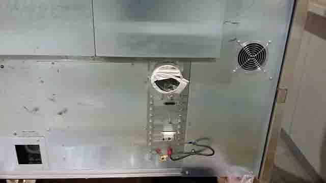

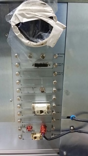

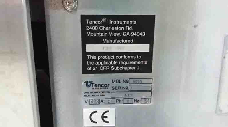


ID: 293595750
Wafer Size: 8"
Vintage: 1997
Darkfield inspection system, 8"
1997 vintage.
KLA / TENCOR AIT (Advanced Inspection Technology) is a wafer testing and metrology equipment for semiconductor manufacturing. It provides a fast, accurate, and efficient way to measure and analyze defects during wafer fabrication and packaging processes. This high-precision system is capable of performing a wide variety of wafer testing, metrology, and inspection tasks, including optical inspection, electron beam imaging, laser diffraction, transmission electron microscopy (TEM), resist density measurement, particle detection, cryo-sample imaging (CSI), burn-in test, and automated defect review (ADR). The unit's inspection capabilities range from investigating distinctive surface features of wafers, detecting extremely small particles is found on the sample, to complete performance analysis of chips. The integrated detection solutions deliver considerable improvement in throughput and time savings, while providing exceptionally precise results. It also offers image analysis automation, which provides repeatable and reliable metrics that support process optimization. The machine enables fully automated scanning, particle detection, and total inspection of all stages of a wafer's production process, from development to fabrication. This ensures that the final products meet the OEM's quality criteria, for maximum reliability and performance. The tool incorporates high-speed, high-accuracy, automated focusing, and SEM scanning to deliver comprehensive defect inspections, meeting a wide range of wafer technologies from photovoltaic cells to memory device fabrication. In addition to automated wafer testing, the asset provides a host of other capabilities. It supports both manual and fully automated sampling, with results that are instantly available for presentation and analysis. It can also be optimized to identify potential sources of contamination and clusters of defects at each stage of the fabrication process, ensuring total process control. It also enables positive product identification and tracing for traceability purposes. By providing this level of accuracy, performance, and automation, KLA AIT model enables semiconductor manufacturers to maximize their yields, reduce product costs and optimize their total production costs. The results are a more competitive and efficient production line, ensuring that their products exceed industry standards and customer expectations.
There are no reviews yet

