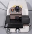
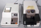
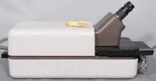
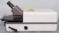
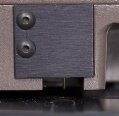
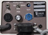
Used KLA / TENCOR Alpha Step 100 #9016122 for sale
URL successfully copied!
Tap to zoom




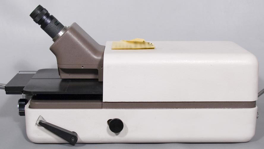

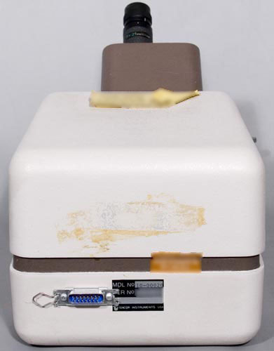

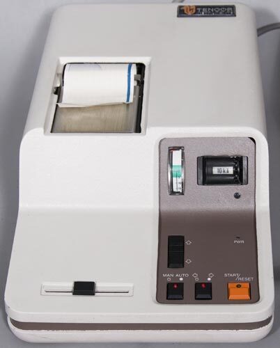

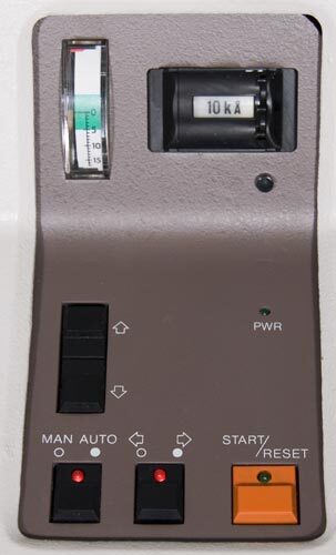





ID: 9016122
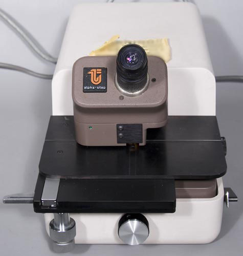
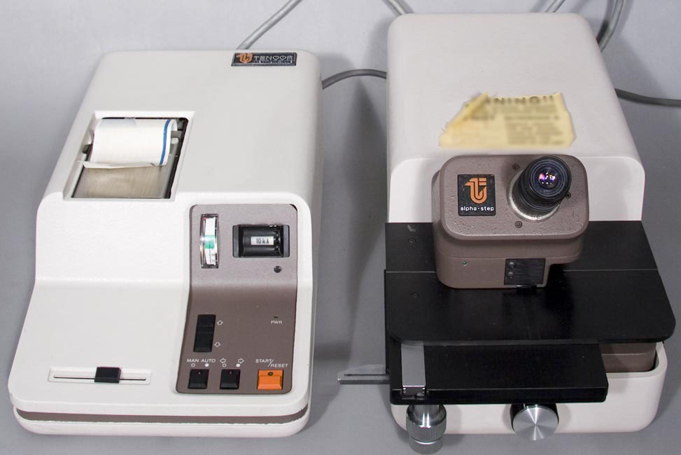
Profilometer / Surface profiler
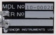
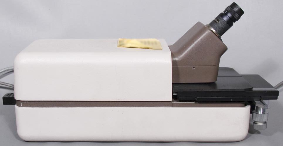
Scan unit:
Model number: 10-00020
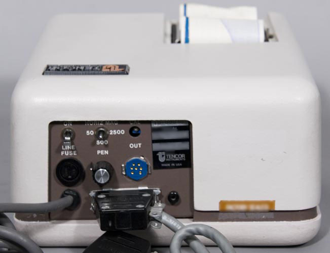
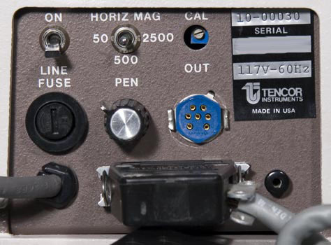
Controller unit:
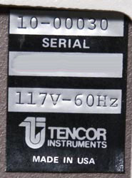
Model number: 10-00030
Power requirements: 117 V - 60 Hz
Features:
Automatic leveling
Measurements completed in less than 1 minute
1,000 Å full-scale
No shock isolation required
Mechanical, electronic and thermal stability
Specifications:
Measurement ranges (full-scale deflection): 1,000 å, 2,500 å, 5,000 å, 10 kå, 25 kå, 50 kå, 100 kå, 250 kå, 500 kå, 1,000 kå
Resolution: 10 å (minimum detectable step)
Auto zero: Recorder automatically starts at any preset level
Horizontal magnification / scan speed / recorder speed:
50 x / 0.1 mm/sec 5 mm/sec
500 x / 0.01 mm/sec / 5 mm/sec
2500 x / 0.01 mm/sec / 25 mm/sec
Scan length: 3 mm in either direction (6 mm total)
Stylus: diamond 12.5 µ radius standard
Tracking force: Factory-set 15-18 mg (1 mg minimum)
Sample stage dimension: 190 mm (7.5") w x 127 mm (5") deep
Sample stage movement:
X-axis: 3 mm (12")
Y-axis: 48 mm (1.9")
Z-axis: 11 mm (46") plus (vertical) stylus lift
Throat depth: 65 mm (2.54") allowing measurement anywhere on a 125-mm (5") Dia wafer
Maximum acceptable sample thickness: 11 mm (46")
Operational modes:
Automatic leveling and scan
Manual leveling and scan
Automatic leveling and manual scan
Optics: Non-inverted image, 22x magnification
Illumination: Light-emitting diodes
Chart recorder:
Type: Thermal printing
Chart speeds: 5 and 25 mm/sec
Chart size: 5 cm (2") Continuous roll
Linearity: ±1% full-scale
Max drift vs temperature: 0.5 division/10°c
Max drift vs time: 0.1 division/8 hrs
Dimensions:
Scan unit: 208 mm (8.2") w x 226 mm (8.9") h x 422 mm (16.6") d
Control unit: 216 mm (8.5") w x 125 mm (4.9") h x 394 mm (15.5") d
Weight:
Scan unit: 7.7 kg (17 lbs)
Control unit: 6.4 kg (14 lbs).
KLA / TENCOR Alpha Step 100 is a wafer testing and metrology equipment that can be used for non-destructive optical measurements and 3D topography of nanometer-scale features. This system enables precision measurement of device structures, multiple patterning layer film thicknesses, and critical dimensions on semiconductor wafers and other substrates. KLA Alpha Step 100 features a scanning tunneling microscope (STM) and a quad-cell interferometer (QCI) to accurately measure a wide variety of parameters. The STM operates in a vacuum environment and allows for imaging of surface features with nanometer-level precision. The QCI measures nanometer-level film thicknesses, in addition to 3D topographical features of wafer surfaces. The unit also boasts a non-contact surface profilometer that captures 3D images of surfaces with 2.5 nanometer image resolution. The profilometer collects both topographical and surface data, in addition to material properties like surface roughness. TENCOR Alpha Step 100 is capable of detecting even the most subtle defects and provides the highest level of accuracy for both wafer measurement and print inspection. It has an advanced phase-shifting analysis program that can detect both over- and under-exposure issues. The machine also includes an analysis package for measuring critical dimensions and addressing line width, line edge roughness, line and space width variation, and overlay between layers. Alpha Step 100 can be integrated with measurement tools for additional applications such as process monitoring and yield analysis. Additionally, this tool can be used with an autostage feature to enable high throughput testing. The asset is also equipped with a computer-controlled optical head that allows for non-contact multi-sample alignment and measurement, enabling high-precision testing in a single pass. The model enables full 3D topographical imaging without the need for planar or wafer-level focus correction. This is crucial for both wafer qualification and monitoring process drift from tool-to-tool and through process runs. Additionally, KLA / TENCOR Alpha Step 100 features a programmable wafer stage, with multiple samples oriented in different configurations to optimize throughput and accuracy for different die sizes, making it very useful for semiconductor wafer testing.
There are no reviews yet
