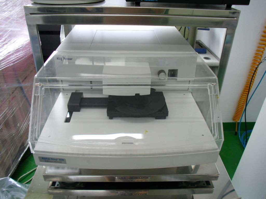
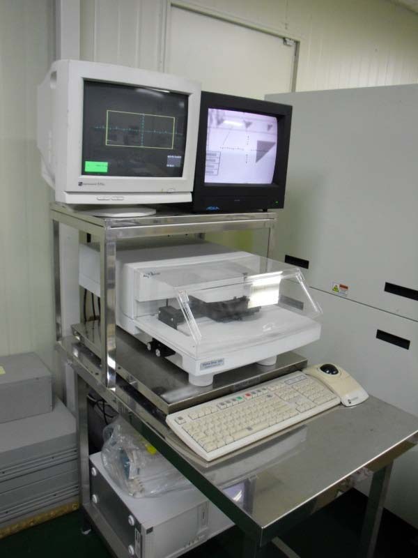
Used KLA / TENCOR Alpha Step 500 #9084578 for sale
URL successfully copied!
Tap to zoom


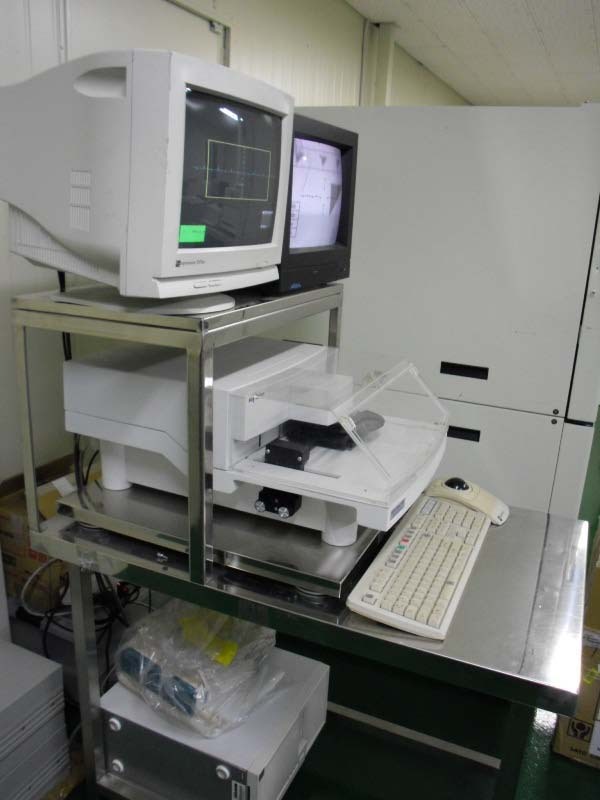




ID: 9084578
Vintage: 2000
Surface profiler
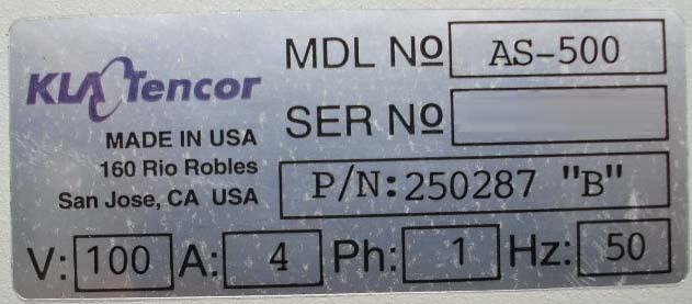
P/N: 250287 "B"
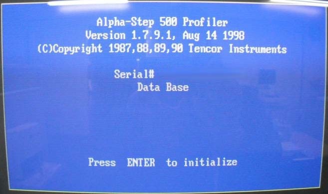
OS Version: MS-DOS 6.22
Software version: Ver. 1.7.9.1
2000 vintage.
KLA / TENCOR Alpha Step 500 is an advanced wafer testing and metrology equipment designed to measure the thickness, composition, geometric profile, and electrical properties of a variety of materials, including semiconductor, optoelectric, and micromechanical components. This system combines optical interferometry, infrared spectroscopy, and capacitance-voltage techniques to collect data on a wide range of substrates. Using its very precise, three-dimensional optical focus technique, KLA Alpha Step 500 measures the thickness of nearly any material down to a fraction of a nanometer in accuracy. This allows it to simultaneously measure the composition and composition distribution of the wafer material as well as test its electrical properties, such as resistance and current leakage characteristics. This allows the unit to detect the bad batches and measure the roughness variations of the wafers. TENCOR ALPHASTEP 500 utilizes high-performance infrared spectrometers and capacitance-voltage data acquisition systems to characterize semiconductor and optoelectronic wafers. This machine can identify various compound semiconductor material systems, such as silicon germanium, gallium nitride, and silicon carbon nitride, and measure their substrate surface composition distributions with a sub-monolayer resolution. Additionally, KLA / TENCOR ALPHASTEP 500 is capable of real-time positioning of the optical field of view, allowing for an accurate measurement of composition and thickness of the layer. KLA ALPHASTEP 500 requires a cleanroom environment in order to properly perform all measurements. This tool also features a reliable automation platform with a robotic arm equipped with different probes. This ensures a repeatable measurement of the substrate properties and enables high throughput analysis. Alpha Step 500 is ideal for material research and development, as well as for process and quality control in semiconductor and optoelectronic fabrication lines. This asset is also an advanced tool for characterization and analysis of ever-shrinking, high-complexity microelectronic components.
There are no reviews yet
