Used KLA / TENCOR Candela 6100 #293597437 for sale
URL successfully copied!
Tap to zoom
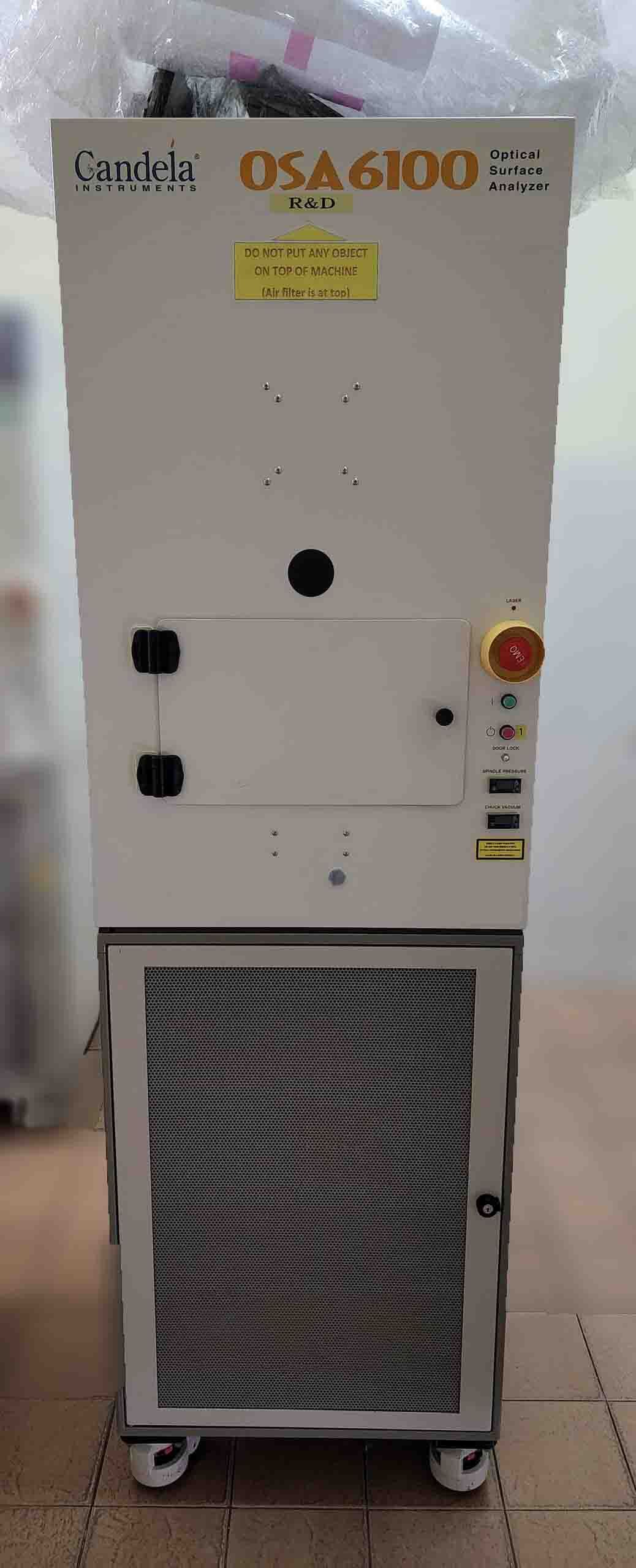

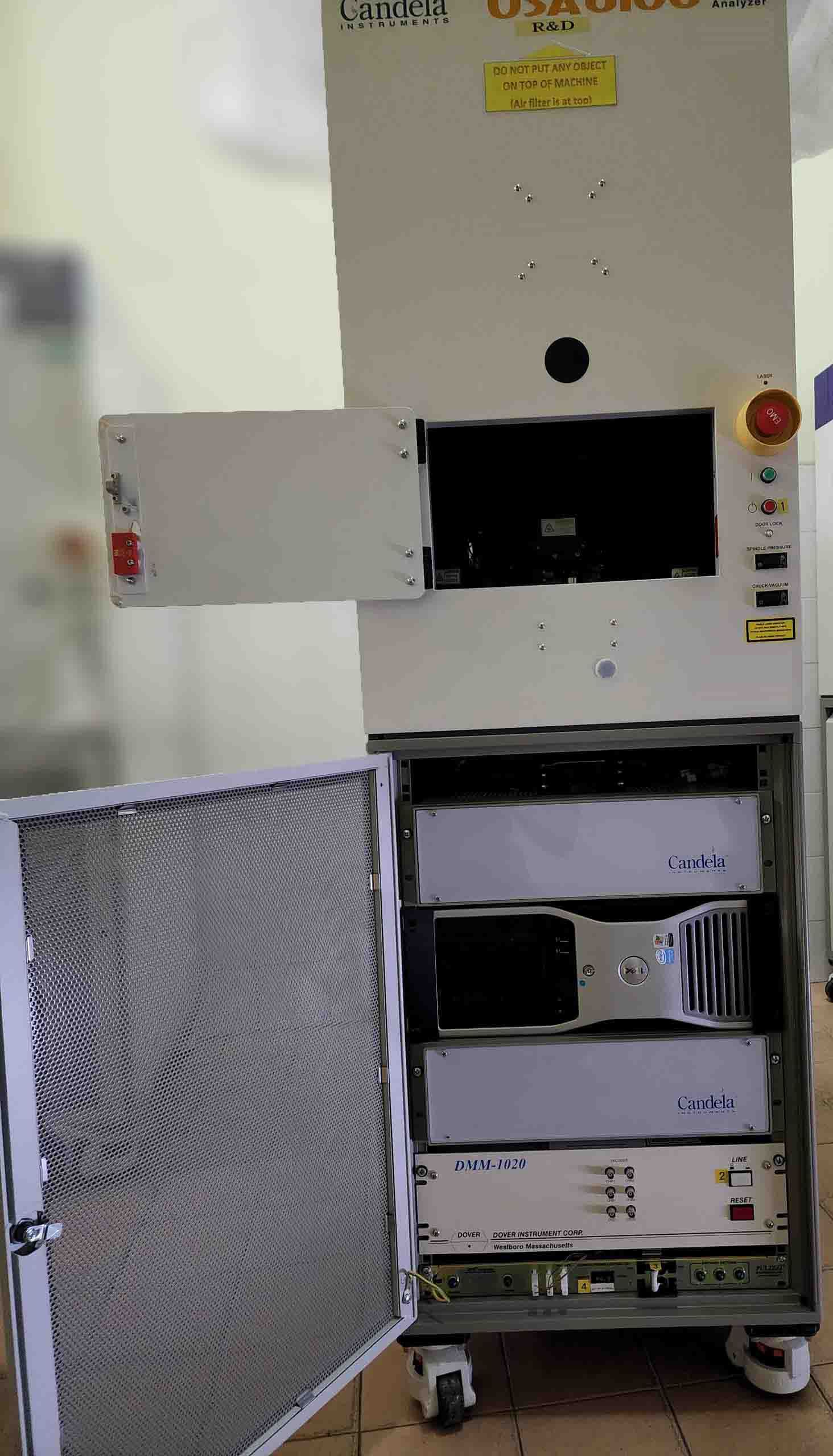

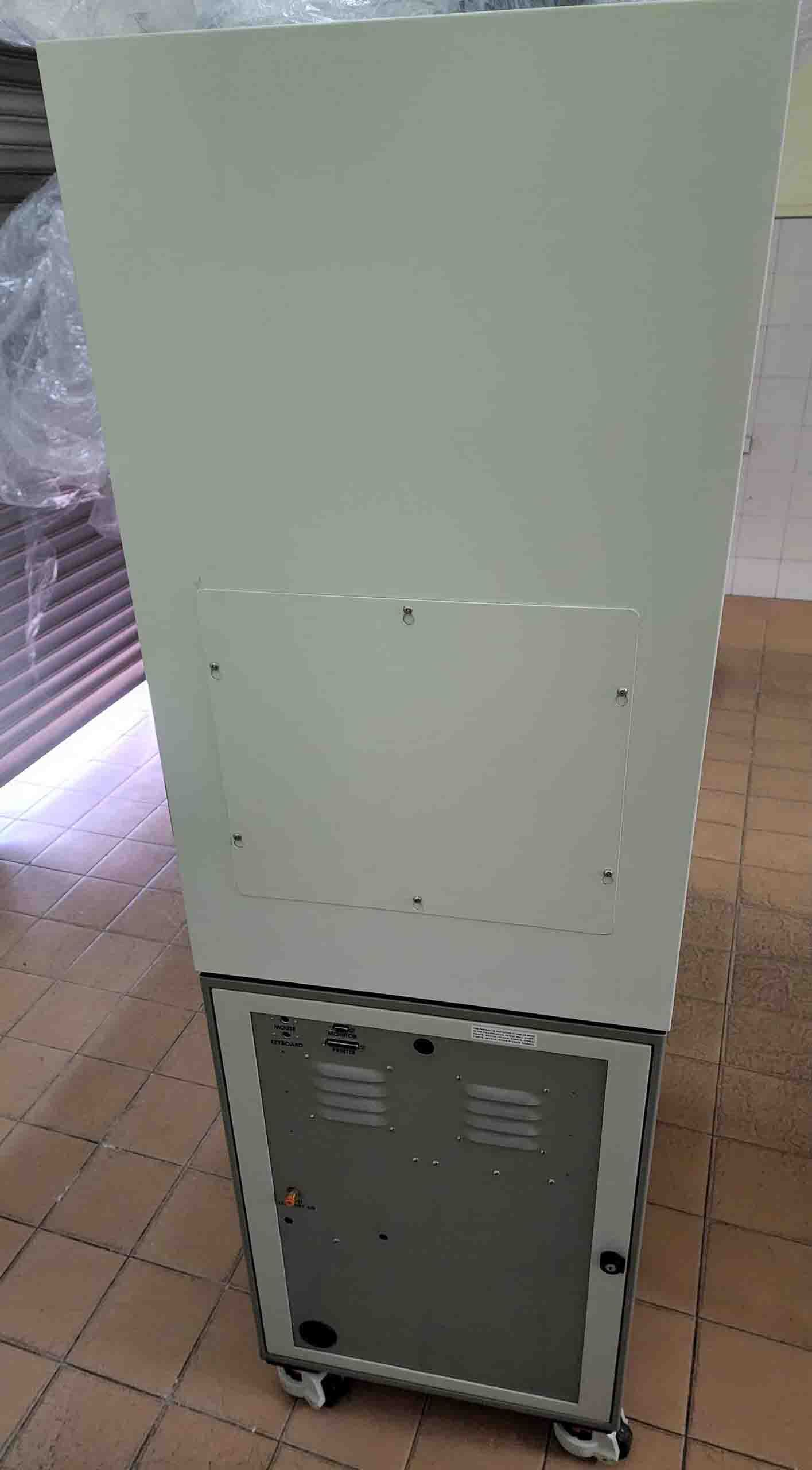

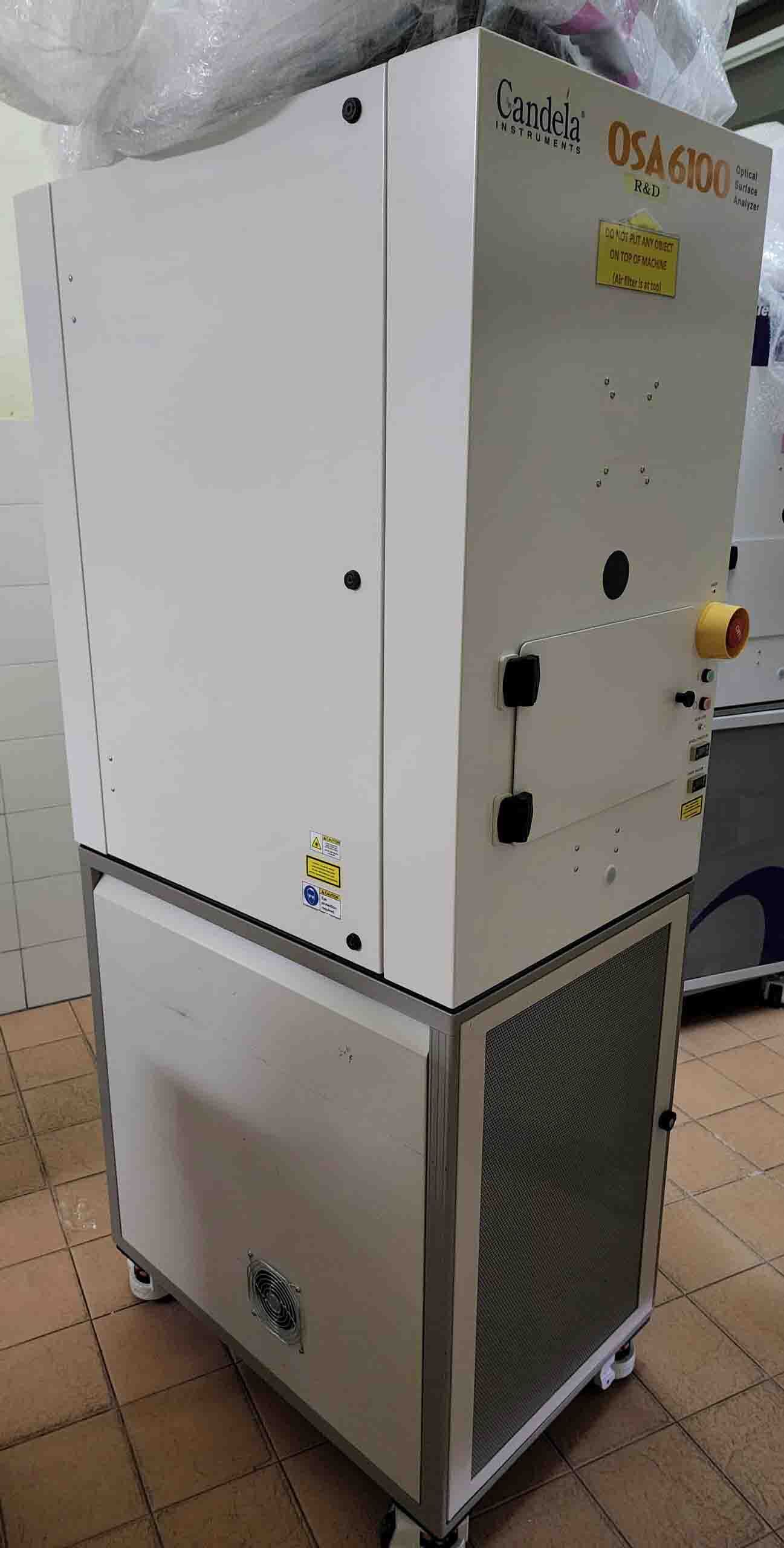

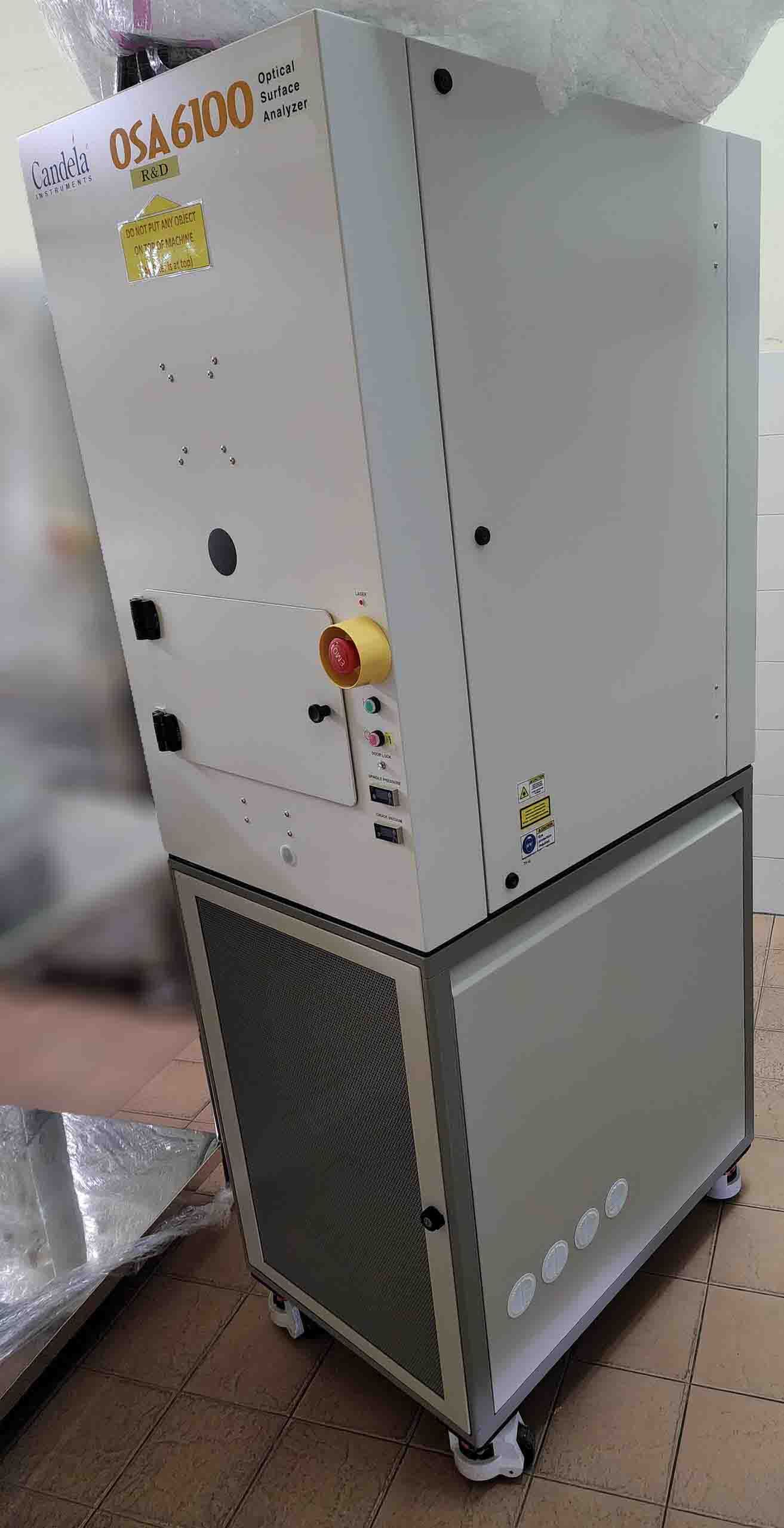

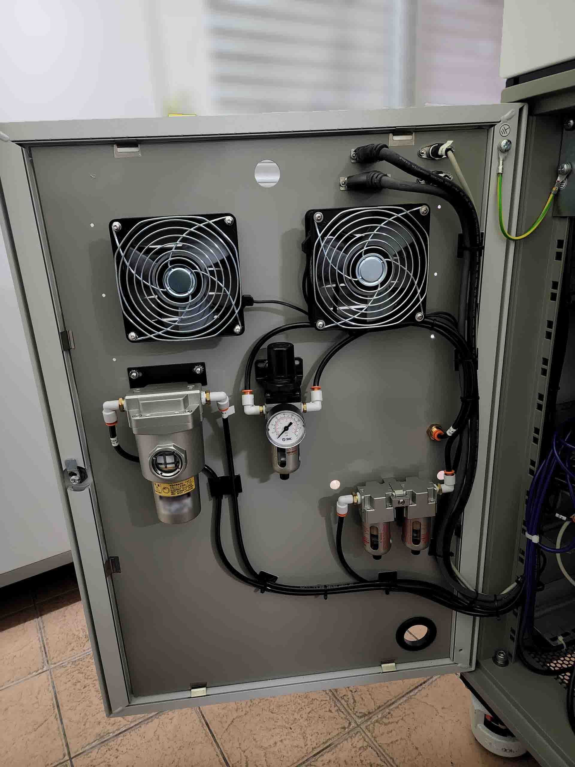

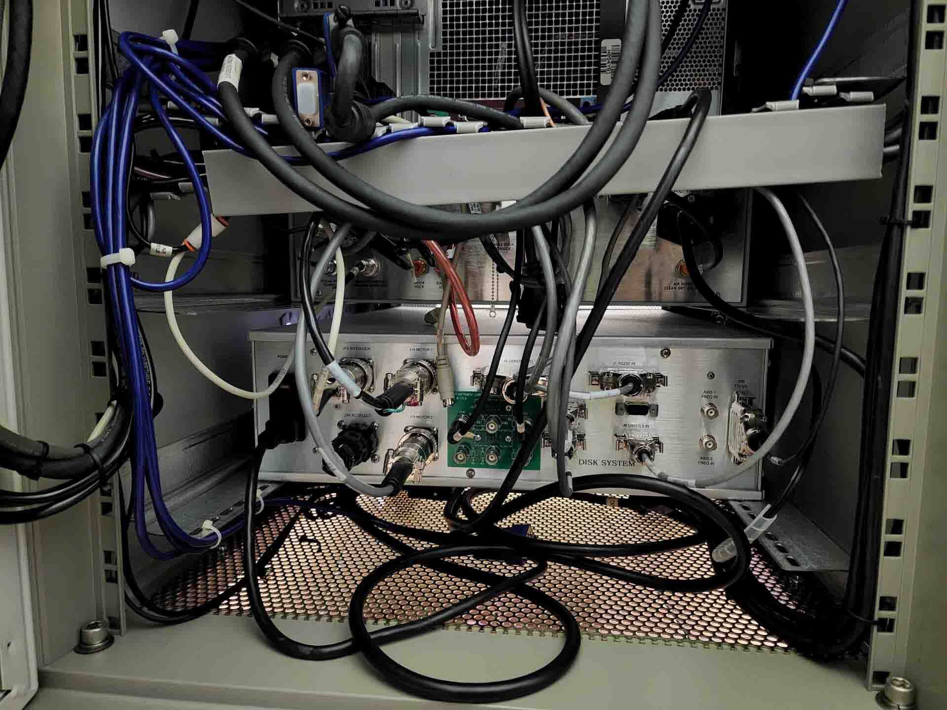

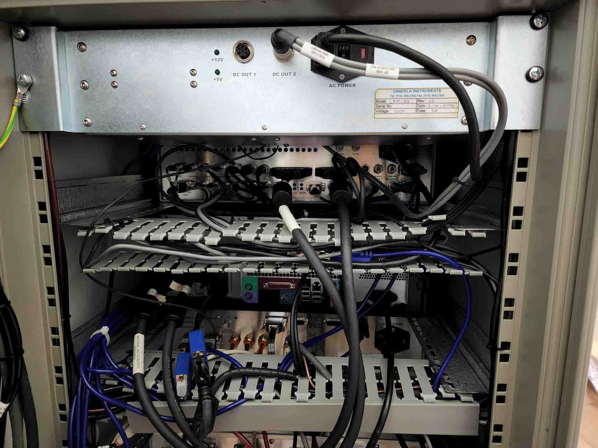

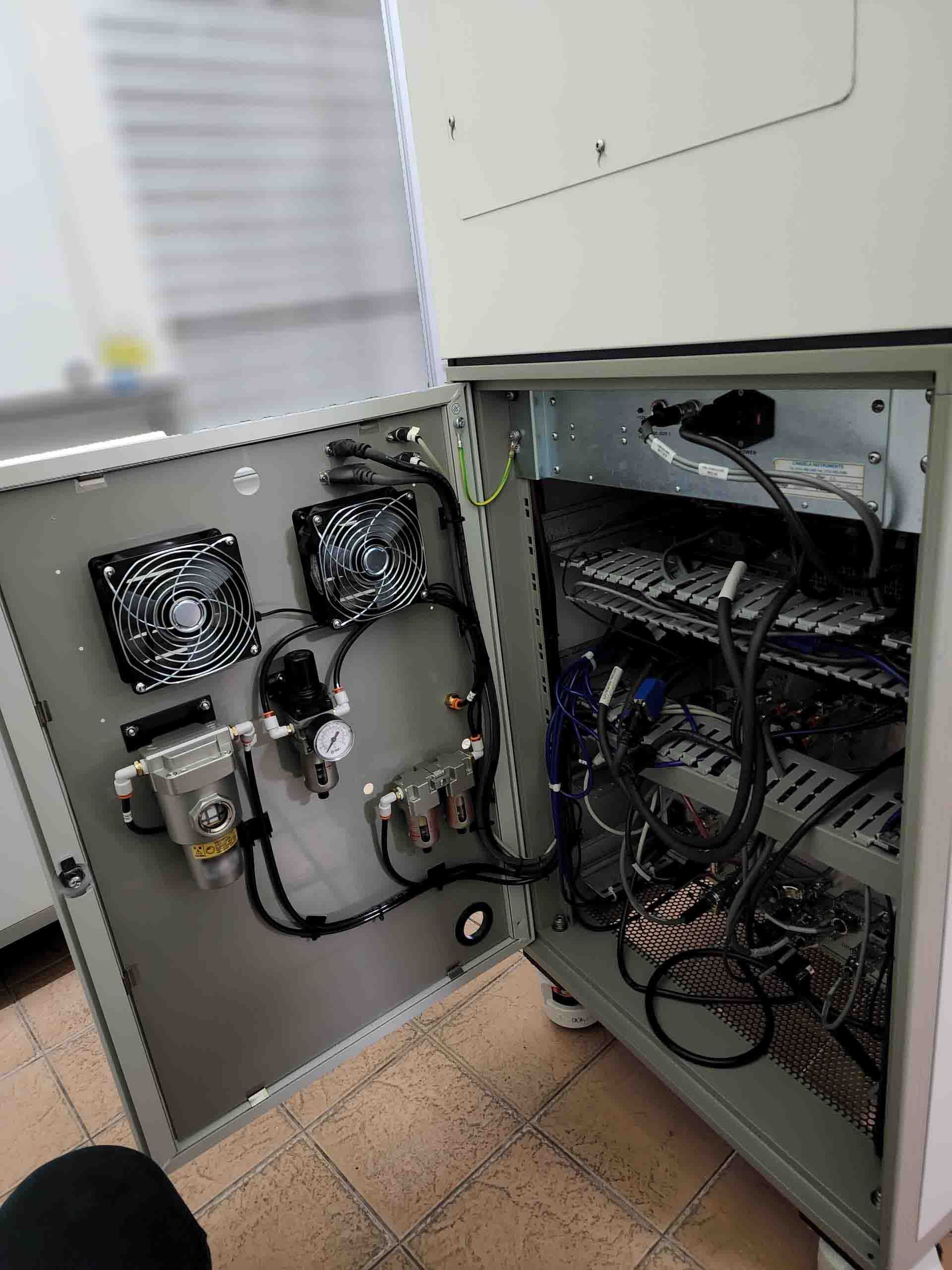

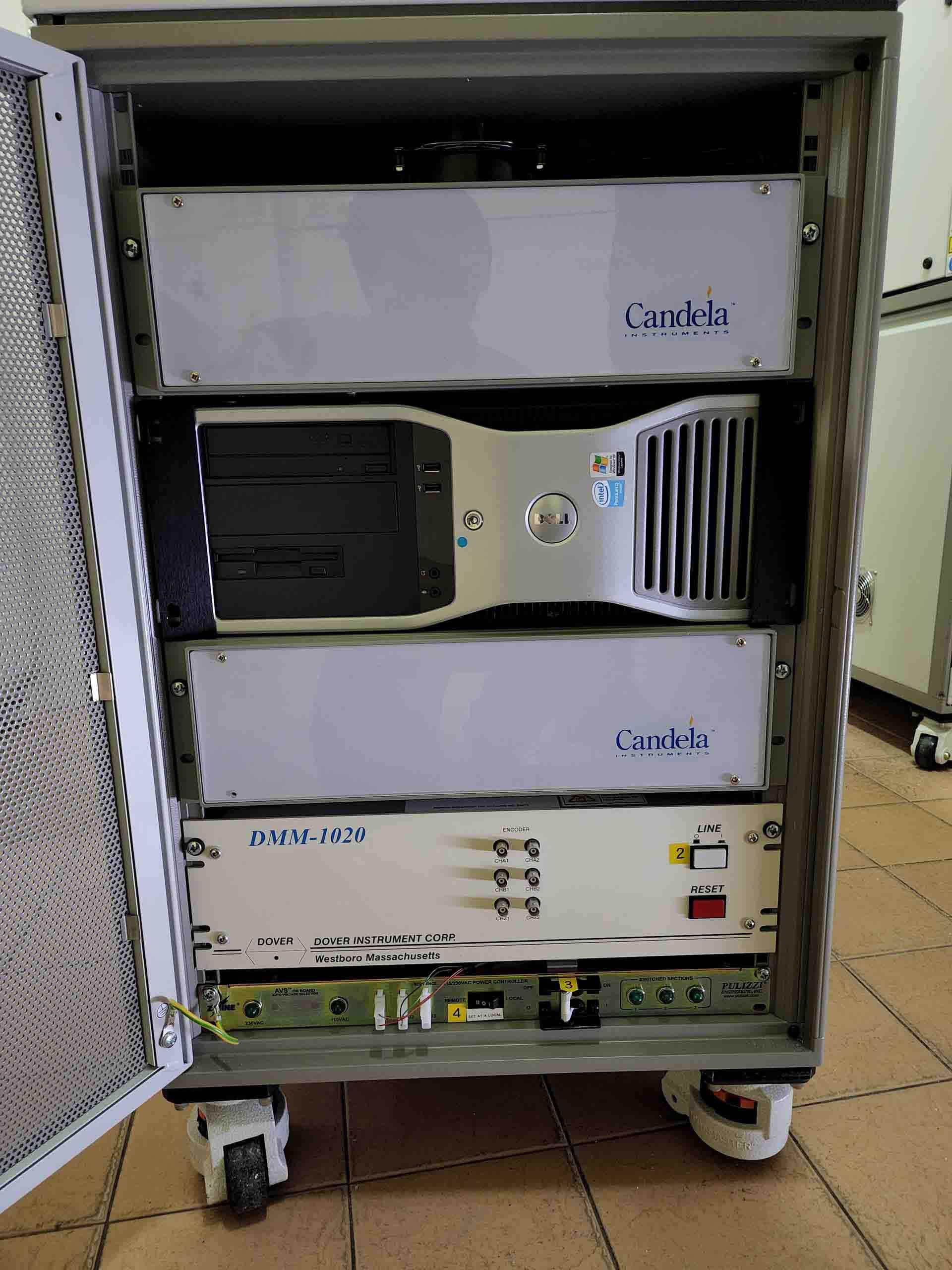



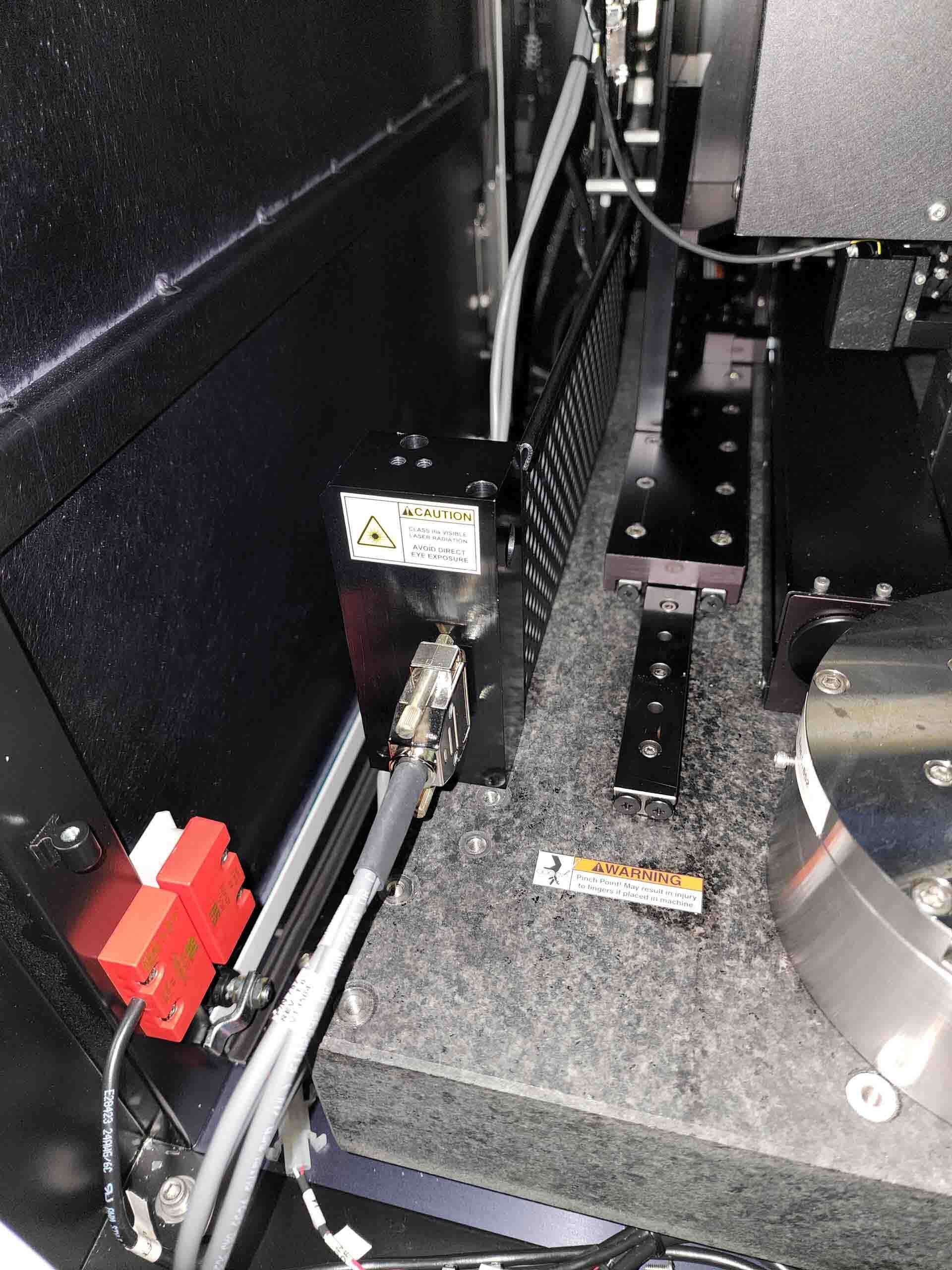

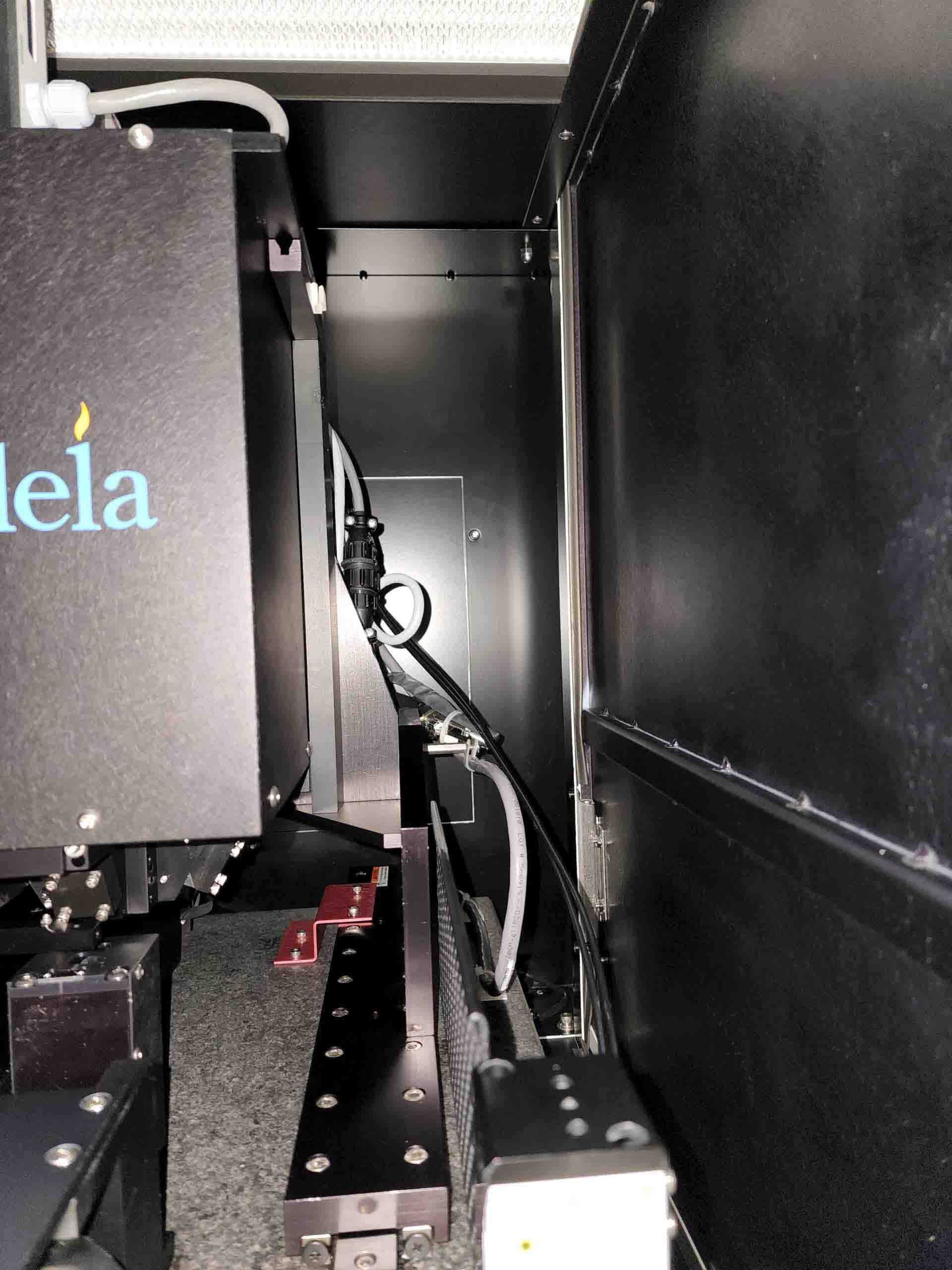

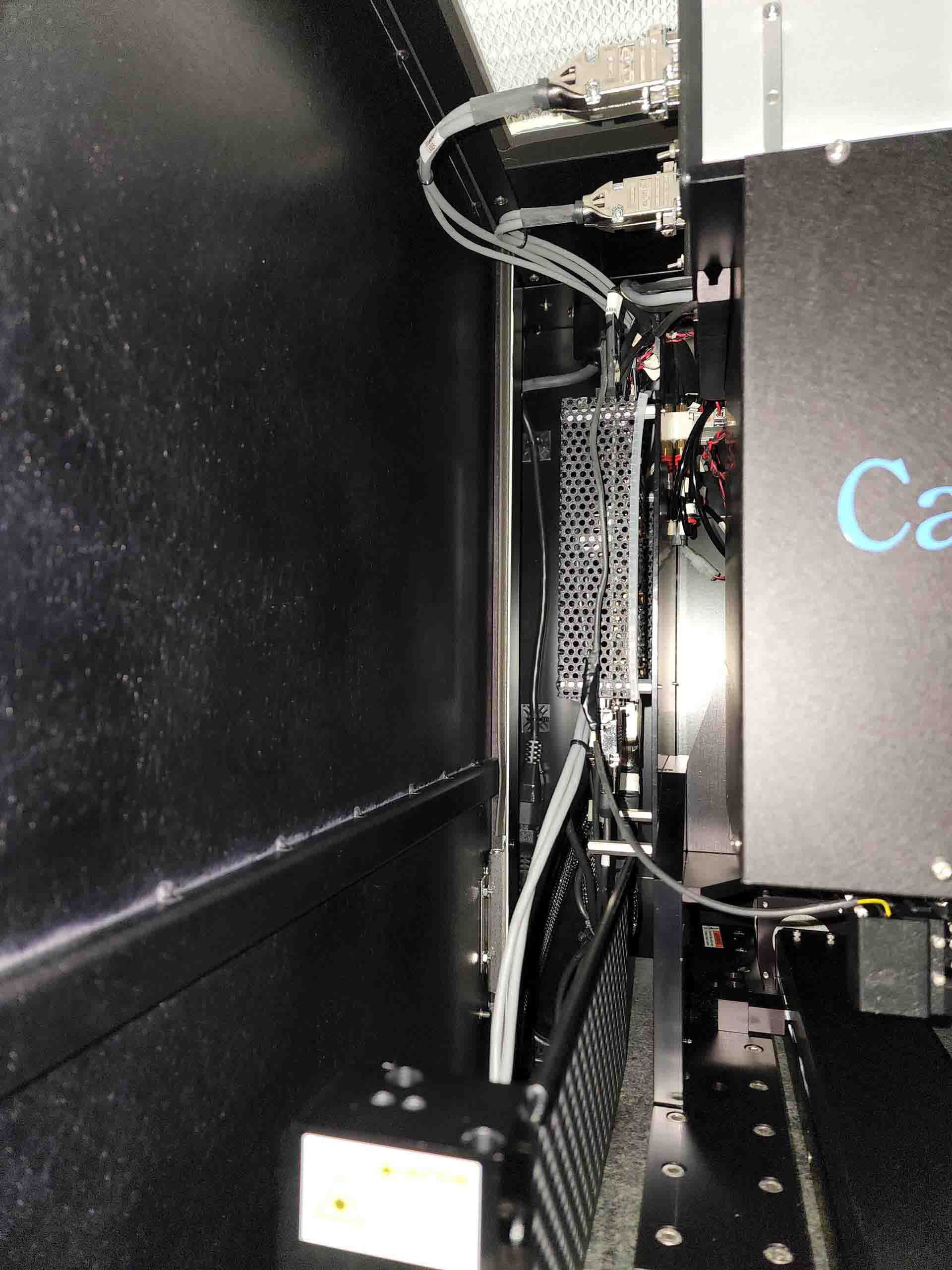

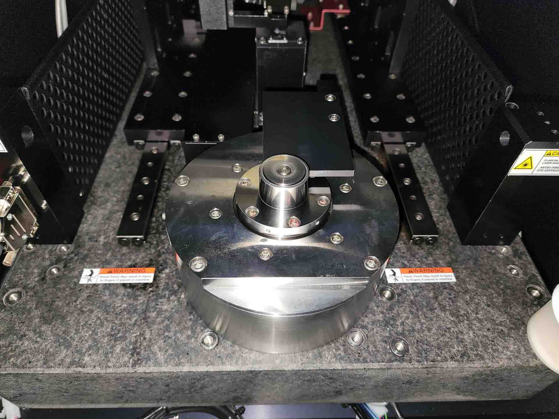

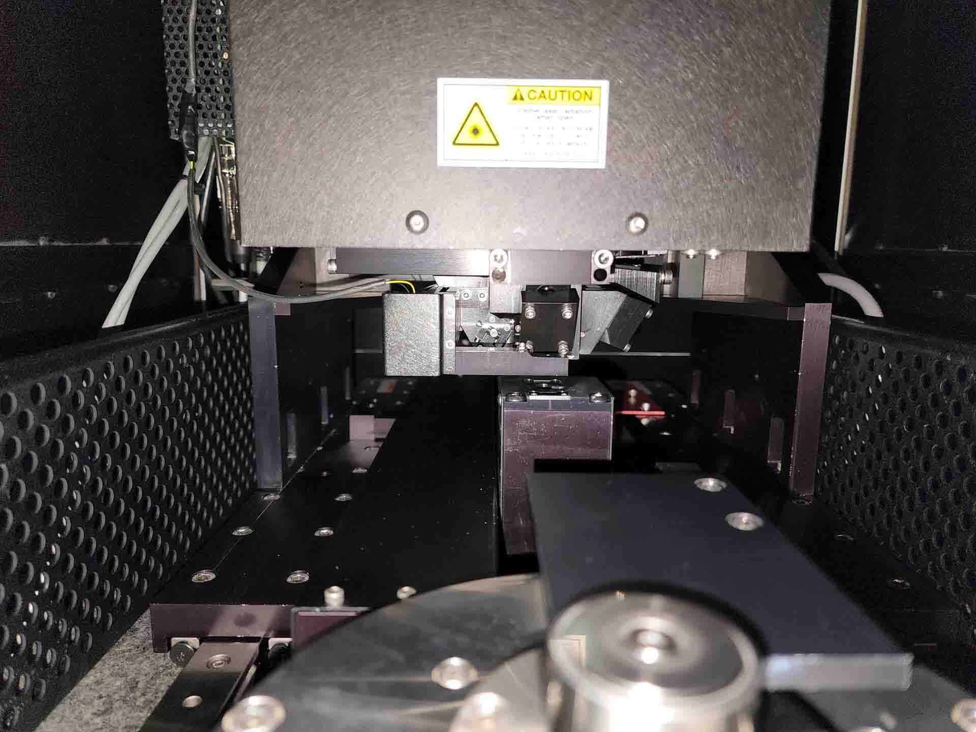

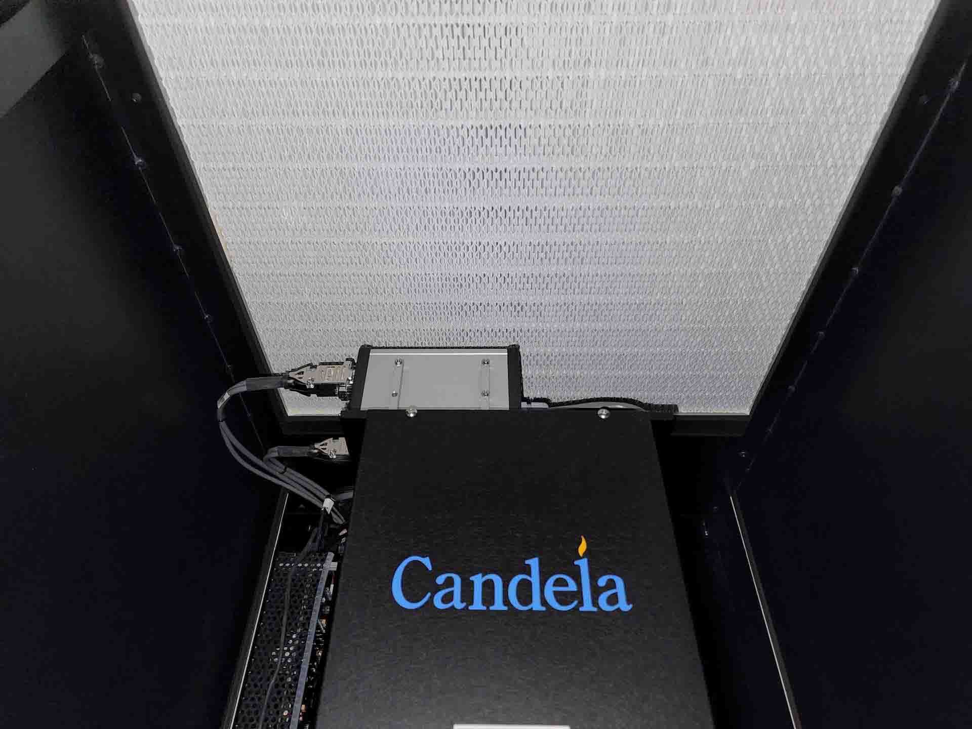

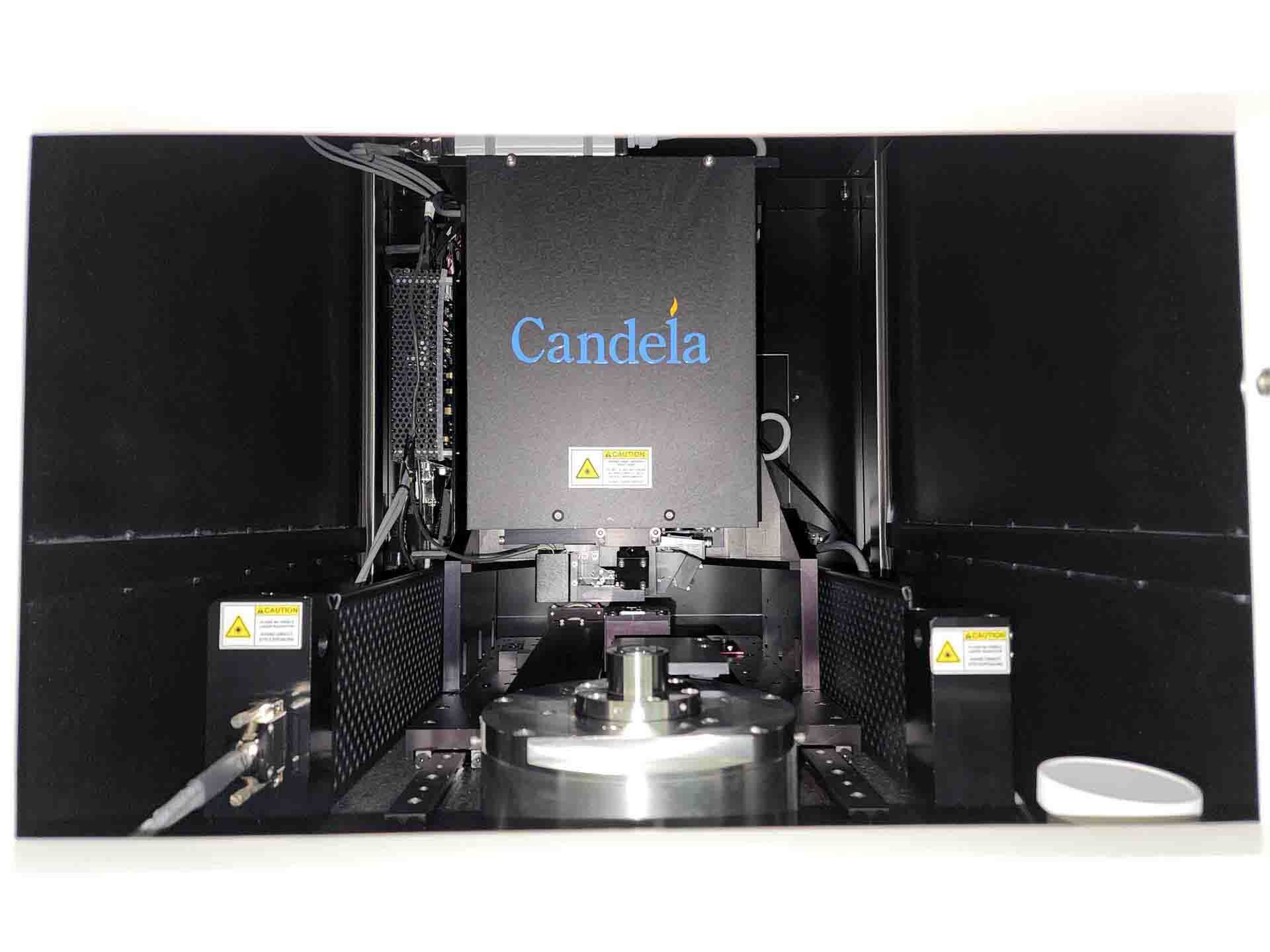

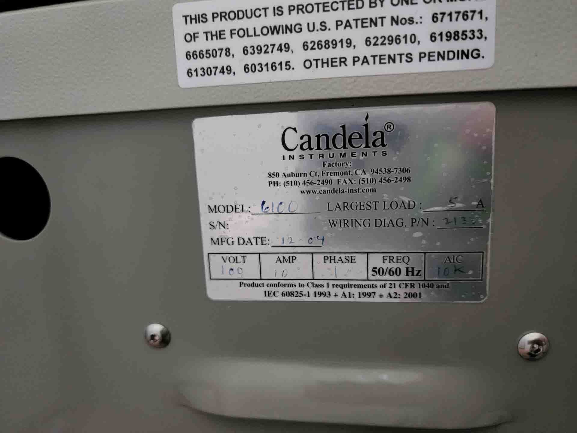

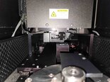
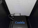
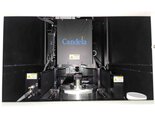
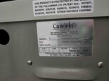
KLA / TENCOR Candela 6100 is a wafer testing and metrology equipment designed to provide accurate and repeatable measurements of the physical characteristics of wafers produced in semiconductor fabrication plants. The system is equipped with a full-field, variable-source photometric imaging unit, a full-field high-magnification microscope, and a 3D laser profiler. This powerful combination of imaging and metrology capabilities offers users an effective tool for wafer process control. The full-field imaging machine is capable of capturing a complete image of the wafer with both brightfield and darkfield illumination. The brightfield imaging helps reveal topographic defects, while the darkfield imaging reveals particles or particles that may not be detectable under normal inspection. Additionally, the imaging tool can detect the presence of mark defects, up to a minimum size of 1.5 microns, as well as detect coating losses on the wafer surface. The full-field high-magnification microscope allows you to identify and measure key parameters such as overlay targets and critical dimensions. The microscope is equipped with a 10x to 100x zoom lens, working distance of 400mm, and three different lighting modes - Off/On/Laser — for identifying different parameters. Through automated scanning, it can also provide an analysis of the entire wafer surface, allowing for more accurate measurements. The 3D laser profiler is useful for verifying the accuracy of metal and dielectric layers. The profiler is equipped with two laser sources, two linescanners, and two cameras. The laser source is used to measure the thickness, etch rate, line width, and surface topology of the layers while the linescanner is used to measure line width, line edge roughness, and profile. The profiler can measure wafers up to a thickness of 760 microns and a diameter of 200mm. Overall, KLA Candela 6100 is a state-of-the-art wafer testing and metrology asset that enables precise measurements of physical characteristics of semiconductor wafers. With its powerful imaging and metrology capabilities, users can confidently track their process performance, verify the accuracy of their product, and ultimately improve their yield.
There are no reviews yet


