Used KLA / TENCOR Flexus 2320 #293724377 for sale
URL successfully copied!
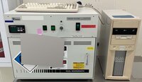
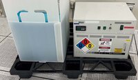
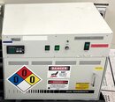
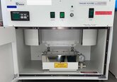
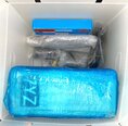
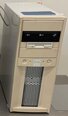
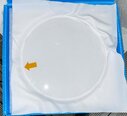
Tap to zoom
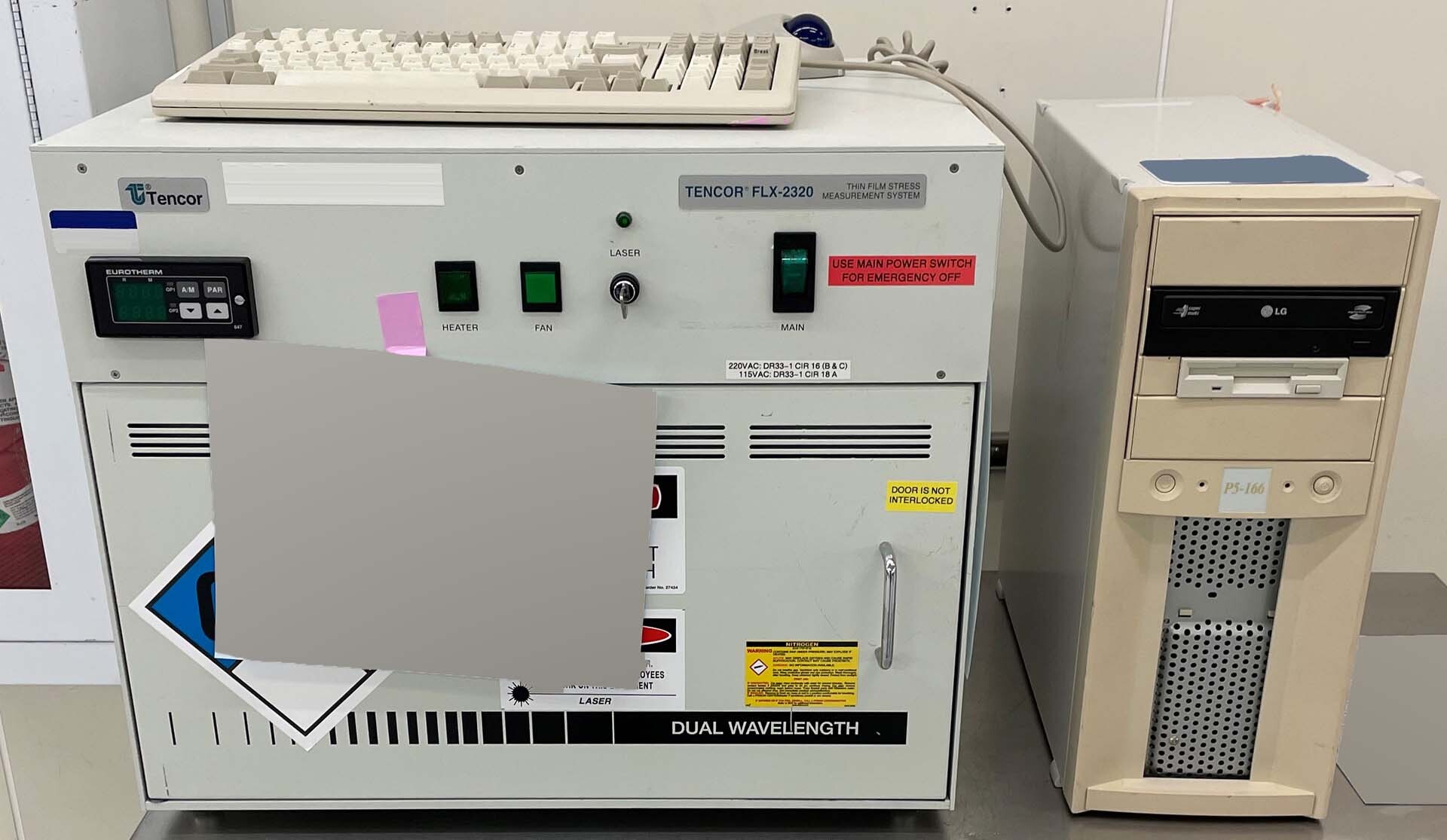

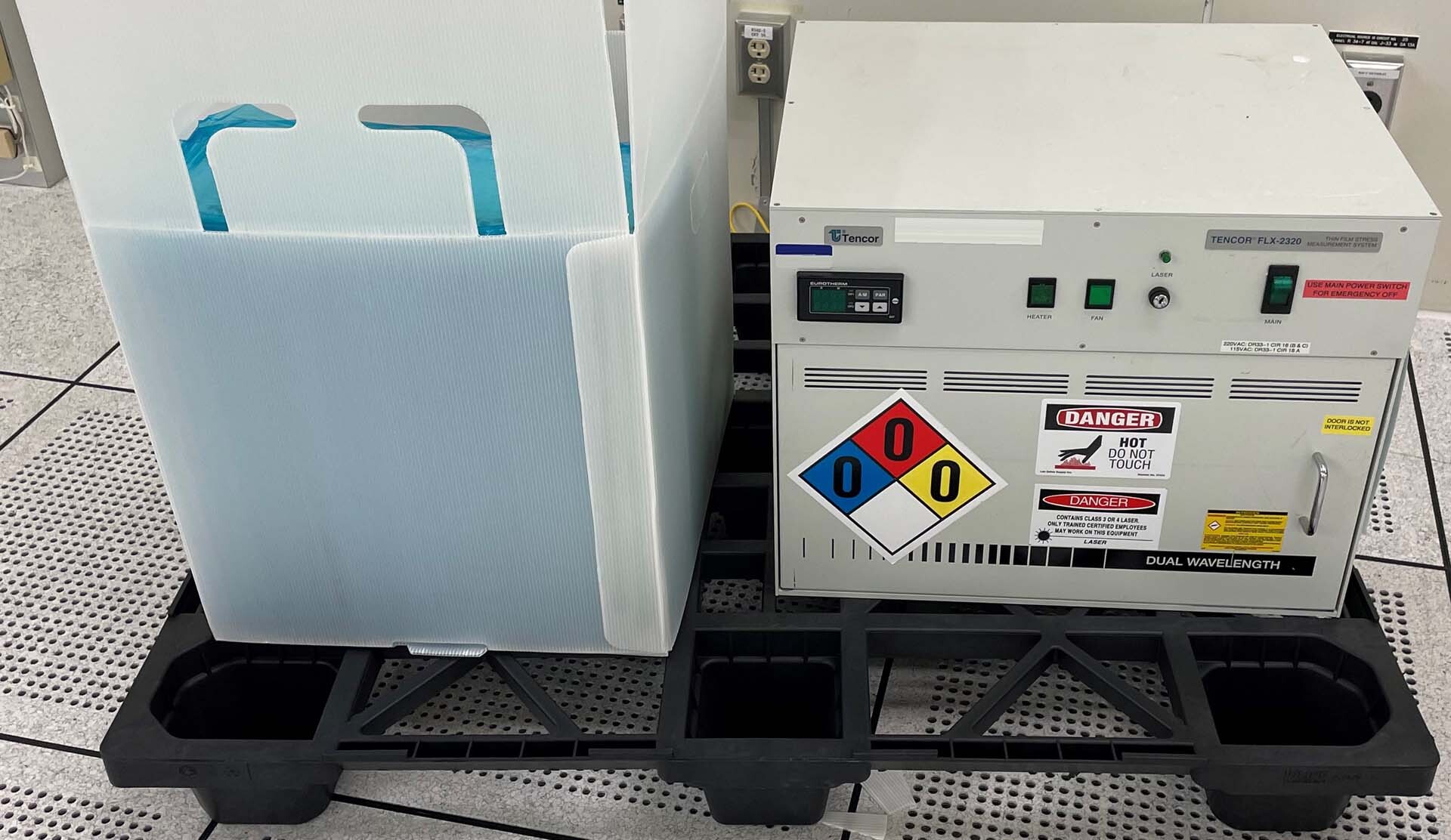
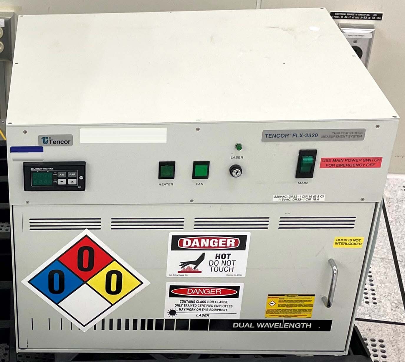
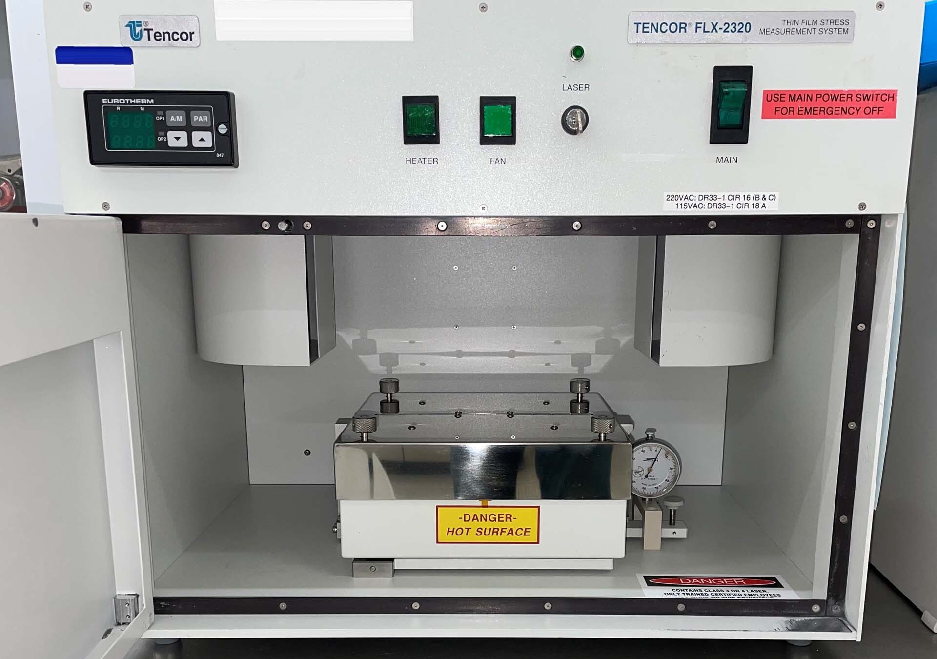
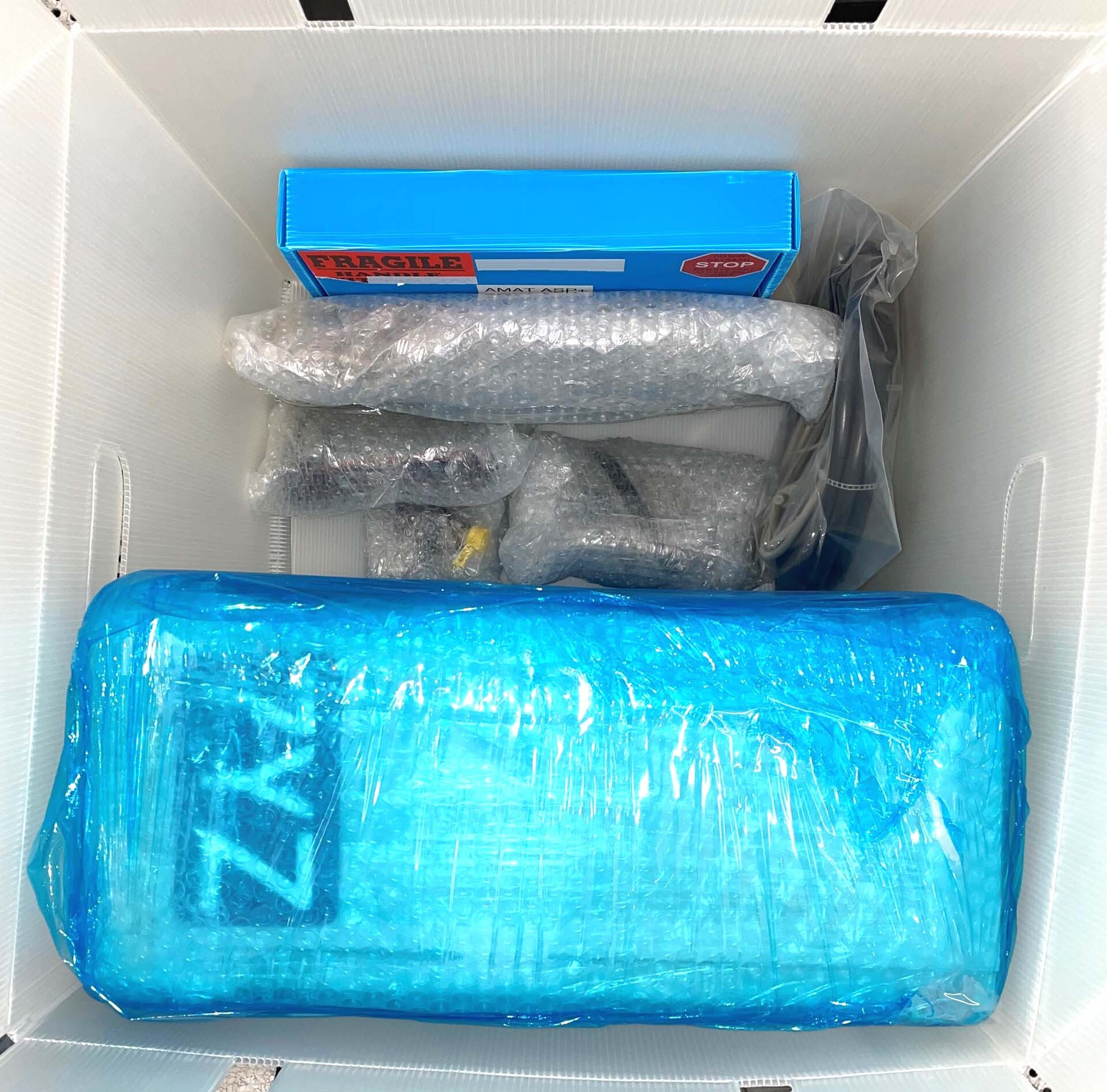
ID: 293724377
Vintage: 2000
Thin film stress measurement system
Stress mapping tool, 8"
Single wafer
Manual loader
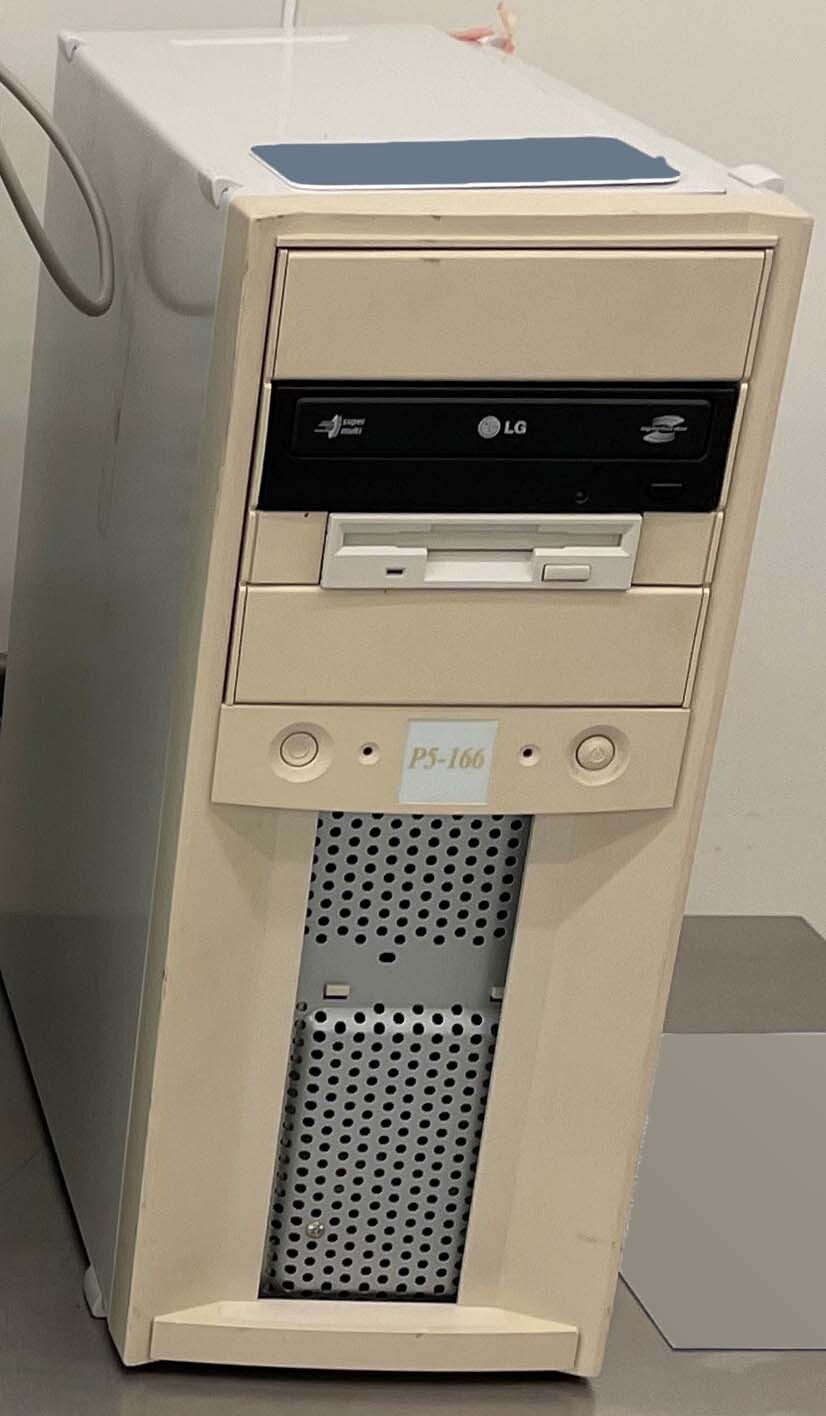
PC: Relay logic
2000 vintage.
KLA / TENCOR Flexus 2320 wafer testing and metrology equipment is a state of the art system utilized in the semiconductor industry. It is designed to test the electrical, visual and dimensional properties of wafers and other large samples in a high-precision environment. KLA Flexus 2320 unit is composed of two main components: an FTI-100A FlawTec Software based imaging machine, and a fully automated SolsTec Metrology tool, linked together to provide superior automated wafer testing and metrology capabilities to the user. The FTI-100A FlawTec Software asset provides defect signals using highly sensitive optics with sub-micron resolution. It consists of a variety of components including an optics subsystem, a field emission electron microscope, an image capture and image processing subsystem, and defect classification software. The optics subsystem acquires images using a high sensitivity CCTV camera, optics, and a CMOS image detector. The electron microscope allows for the examination of fixed patterns and grids as well as line defects, process variations, and grain boundaries. Once the images are captured, an automated image processing subsystem utilizes a set of algorithms to detect and identify defects. After which, the defect classification software uses custom classification algorithms to categorize the defects. The SolsTec Metrology model includes an automated metrology tool suite used for wafer level planar measurements of critical parameters such as thickness, radius of curvature, flatness, and other surface properties. This data allows for further optimization of semiconductor fabrication processes. The equipment utilizes a high speed linear motor stage offering a range of motion of over 200mm, with velocity of up to 600mm/s. A higher end CCD camera is also utilized to capture images of the wafers and measure features down to 0.04 microns in 2D and 0.1 microns in 3D. The software used for metrology also utilizes a sophisticated "multi-step" approach, meaning it can measure different characteristics over different parts of a wafer. TENCOR Flexus 2320 system provides an efficient unit for wafer testing and metrology. Through its combination of fast and accurate defect recognition, and high-precision metrology capabilities, Flexus 2320 is able to provide manufacturers with data useful for optimizing semiconductor fabrication processes. Its state of the art technology also enables the testing of large wafers in shorter time periods than traditional systems, while still maintaining the same high level of accuracy.
There are no reviews yet