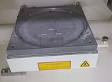
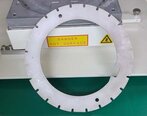
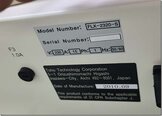
Used KLA / TENCOR FLX-2320S #9303599 for sale
URL successfully copied!
Tap to zoom
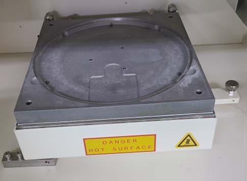

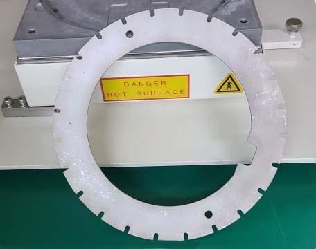

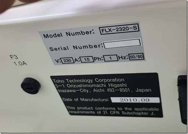

ID: 9303599
Wafer Size: 3"-8"
Vintage: 2010
Stress measurement system, 3"-8"
Scan range: User programmable up to 8"
Minimum scan step: 0.02 mm
Maximum points per scan: 1250
Temperature range: RT to 500°C
Chuck: Heater block
Measurement speed: 6 sec/wafer
Measurement range: 1x10 to 4x10^10 dyne/cm²
Measurement repeatability (1s): 1x10^7 dyne/cm²
Measurement accuracy: <2.5% or 1 Mpa
Minimum radius: 2.0 m
Computer:
Pentium processor 700 MHz
RAM: 128 MB
Hard Disk Drive: 20 GB
Flat panel color monitor, 15"
Operating system: Windows XP
Power requirements: 200-240 VAC, 50/60 Hz, 13 Å
Computer: 115 VAC, 50/60 Hz, 5.4 Å
2010 vintage.
KLA / TENCOR FLX-2320S is an advanced wafer testing and metrology equipment designed for the efficient analysis and characterization of semiconductor devices. KLA FLX 2320 S utilizes an integrated inspection system to detect issues such as chipping, cracking, and stacking which is critical for overall manufacturing and product quality. The unit's advanced metrology capabilities also enable precise measurements of defect size, complexity, and wafer flatness. TENCOR FLX-2320-S is powered by an NXP 32-bit ARM Cortex-A9 RISC processor capable of operating up to 1200MHz. This is coupled to a large-capacity DDR3 RAM and a fast 8GB Flash memory. It also features three high-speed embedded camera systems for capturing full-wafer images as well as zoom-in images of specific defect locations, facilitating resolutions of up to 0.8 microns. FLX 2320 S includes a 255mm open-stage scan platform with integrated motion controllers for high accuracy and repeatability, enabling samples to be accurately tracked during the acquisition process. Additionally, the machine arrives with a high-performance host computer pre-installed with KLA iMapInspect software, enabling operators to make quick, accurate wafer inspections. The tool also supports mapping and analyzing the distribution of defects across an entire 200mm wafer, while simultaneously displaying a false-color image with defect characteristics. In addition, KLA FLX-2320S employs smart automation to streamline the inspection process and offers a wide variety of inspection recipes. These automated recipes allow operators to define repeatable inspection sequences depending on desired criteria, reducing time spent calibrating settings and simplifying batch-to-batch comparisons. The asset accommodates various types of wafer topography, providing a reliable platform for high-volume production of semiconductor devices. Overall, FLX-2320S is an advanced, high performance wafer testing and metrology model that provides comprehensive defect analysis capabilities. Its high-speed embedded cameras and scan stages offer incredible accuracy suitable for any production environment. Together with its outstanding host computer and intelligent automation, the equipment has been optimized to simplify wafer inspection tasks and streamline operations.
There are no reviews yet
