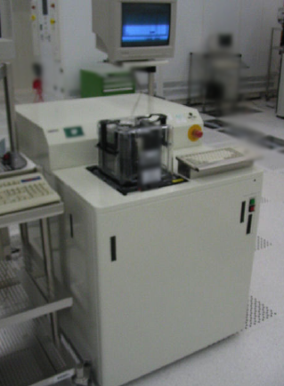
Used KLA / TENCOR FLX-5500 #138548 for sale
It looks like this item has already been sold. Check similar products below or contact us and our experienced team will find it for you.
Tap to zoom


Sold
ID: 138548
Wafer Size: 8"
Vintage: 2003
Stress measurement system, 8"
Sample Handling: 6" & 8"
CE Marked
Standard Specifications:
Throughput: >54 WPH (8")
Measurement:
Speed: 5s (6")
Range: 1x10⁷ to 4x10¹⁰ dynes/cm2
Repeatability: (1σ) < 1x10⁷ dynes/cm2 for 10 measurements
Accuracy: <2.5% or 1MPa (whichever is larger)
Resolution: kmin (1/m) = 0.000100, Kmax (1/m) = 0.400000
Minimum Radious: 3.0m (for 80mm scan length)
Minimum Scan Step: 0.02mm
Maximum Points per scan: 1250
Scan Direction: 15°, 30°, 45°, & 90°
Scan Range: User programmable up to 8"
Detectable Stress: All reflecting films over 1000 Å thick
Process Type: Single Wafer
(1x) Integrated SMIF (Asyst)
Handler Robot: ATM-407B-2-S-CE-S293 (Dual Puck) / Brooks (PRI)
Dual Wavelength Scanning
GEM/SECS Interface
Computer: Pentium 133MHz
16MB Ram
2GB Hdd
SVGA Monitor
OS SW: msWindows 3.11 /DOS 6.22
Application SW: Version 4.3
Power Requirements: V 208-240, Freq 50/60Hz
2003 vintage.
KLA / TENCOR FLX-5500 is an advanced wafer testing and metrology equipment designed to deliver high-throughput integrated analysis solutions to inspect and monitor a variety of wafer characteristics. KLA FLX-5500 is capable of both front-end wafer testing and back-end wafer metrology operations, making it a versatile platform for many applications such as photonics, MEMS, and advanced mobile semiconductors. TENCOR FLX 5500 has two main components: an User Interface/PDU (programmable digital unit) to allow for easy and intuitive user interaction, and a Wafer Metrology System (WMS) featuring integrated optical and RF components to perform operations such as optical inspection, defect analysis, metrology scans, electrical measurements, and other specialized testing. The UI/PDU provides an easy and intuitive way for the user to operate the unit. It includes quick access to control functions such as recipe selection, machine setup, scan control, parameters settings, and data review. The user interface is also capable of modeling real-time performance data, displaying data from multiple perspectives to support faster decision-making. The WMS boasts high-performance optical and RF metrology tools for inspecting and measuring wafer characteristics. The tool integrates several components including a full-spectrum imaging spectrograph to identify and measure light-emitting particles such as cracks and impurities, an auto-focusing imaging asset to check feature sharpness, an automated physical mapping model to monitor the surface of the wafer, and an integrated diamond-turning equipment to precisely measure the surface flatness. In addition, KLA FLX 5500 also includes a powerful software suite with advanced capabilities like automated testing, defect hydration and process control optimization, full hardware monitoring, and robust data security. The software has been designed to maximize the automated testing capabilities of the system, ensuring that each wafer is tested for quality control and process optimization consistently. FLX 5500 is a compact and powerful wafer testing and metrology unit which offers everything needed to test and monitor the quality and performance of any type of wafer. With its intuitive user interface, powerful automated testing capabilities, and integrated optical and RF components, FLX-5500 ensuresand delivers accurate, reliable, and cost-effective results.
There are no reviews yet