Used KLA / TENCOR P-170 #293799729 for sale
URL successfully copied!
Tap to zoom
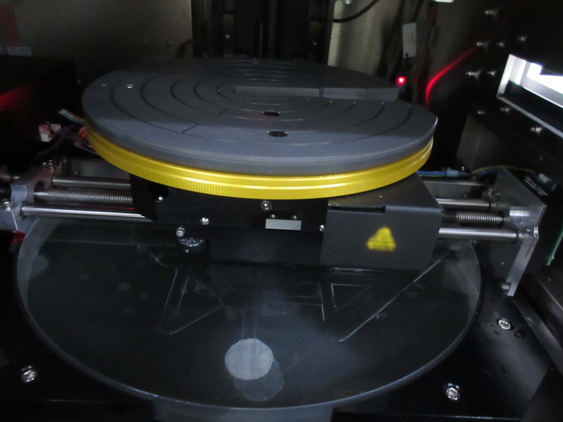

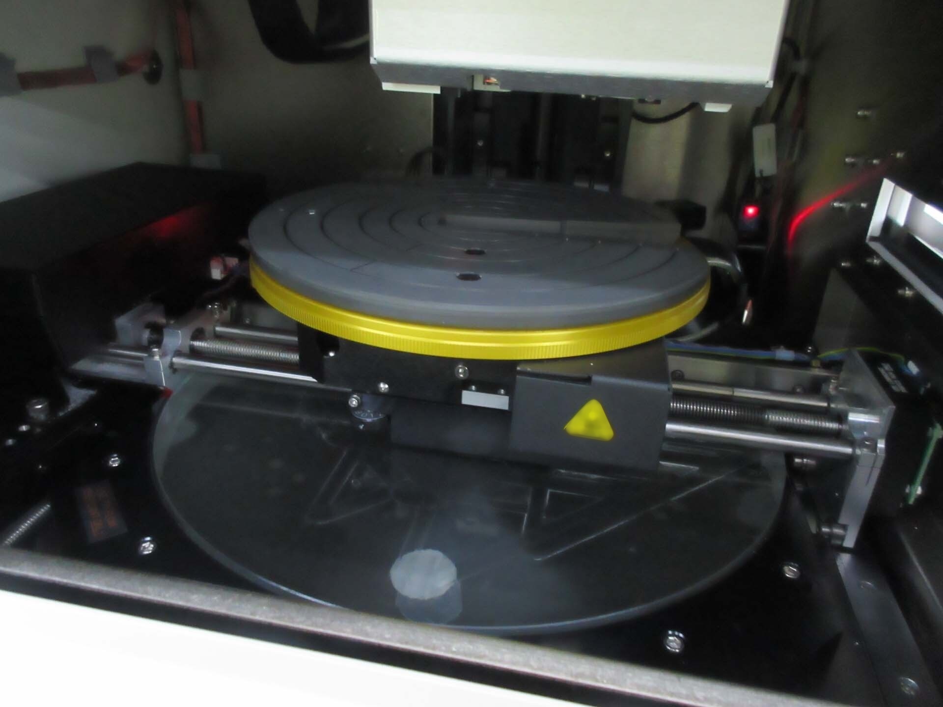
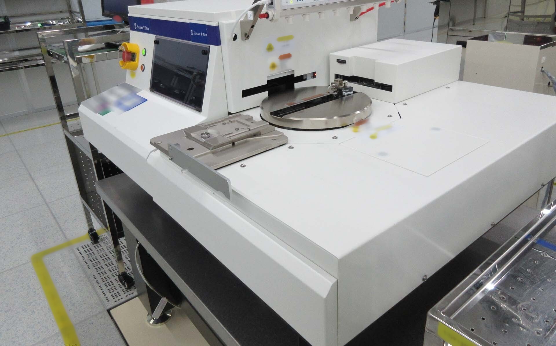
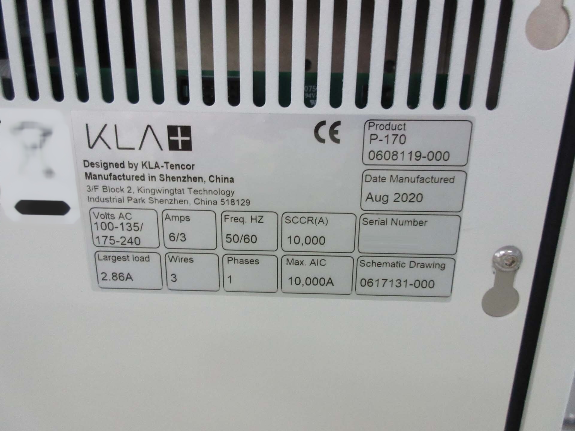
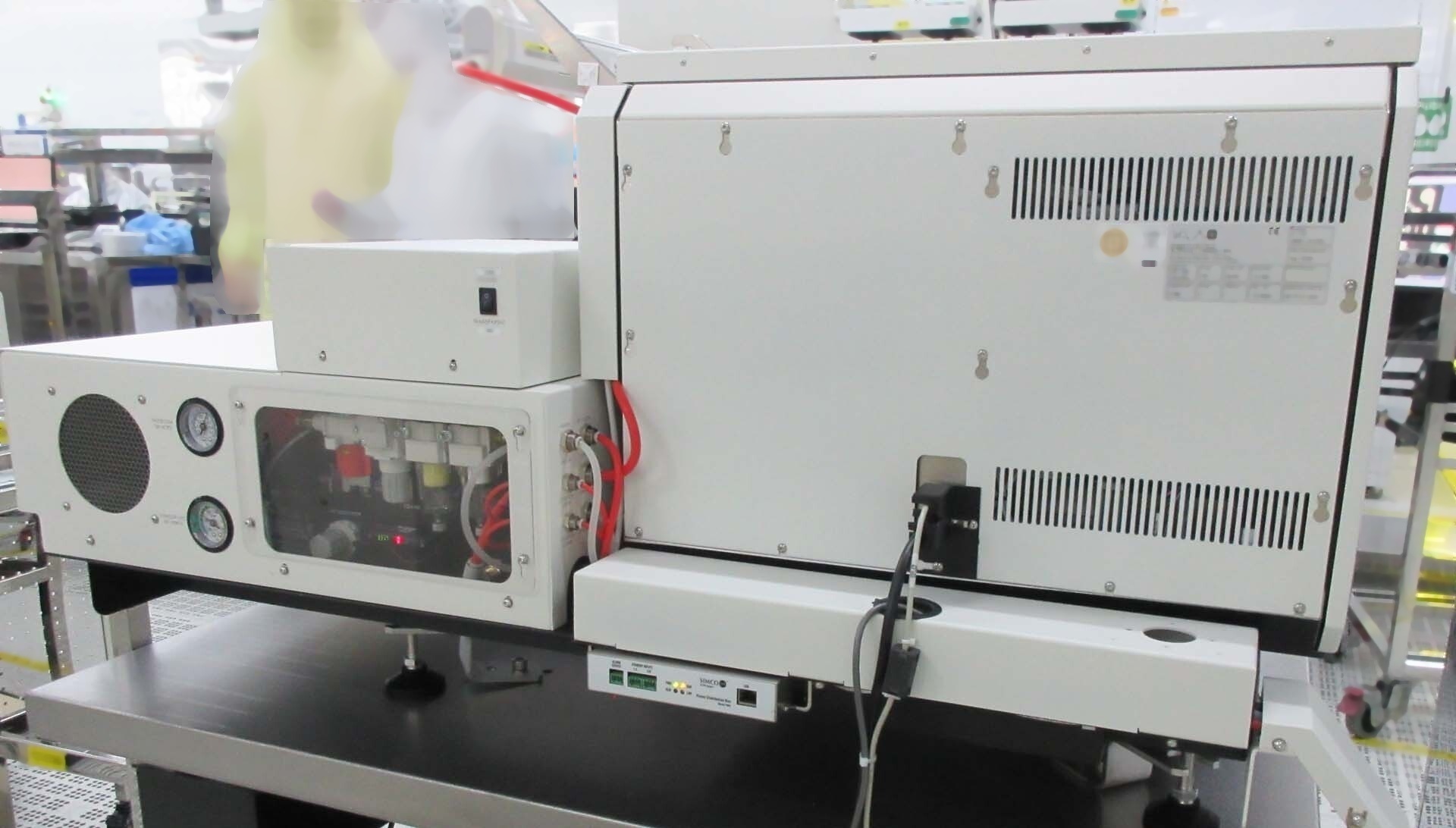
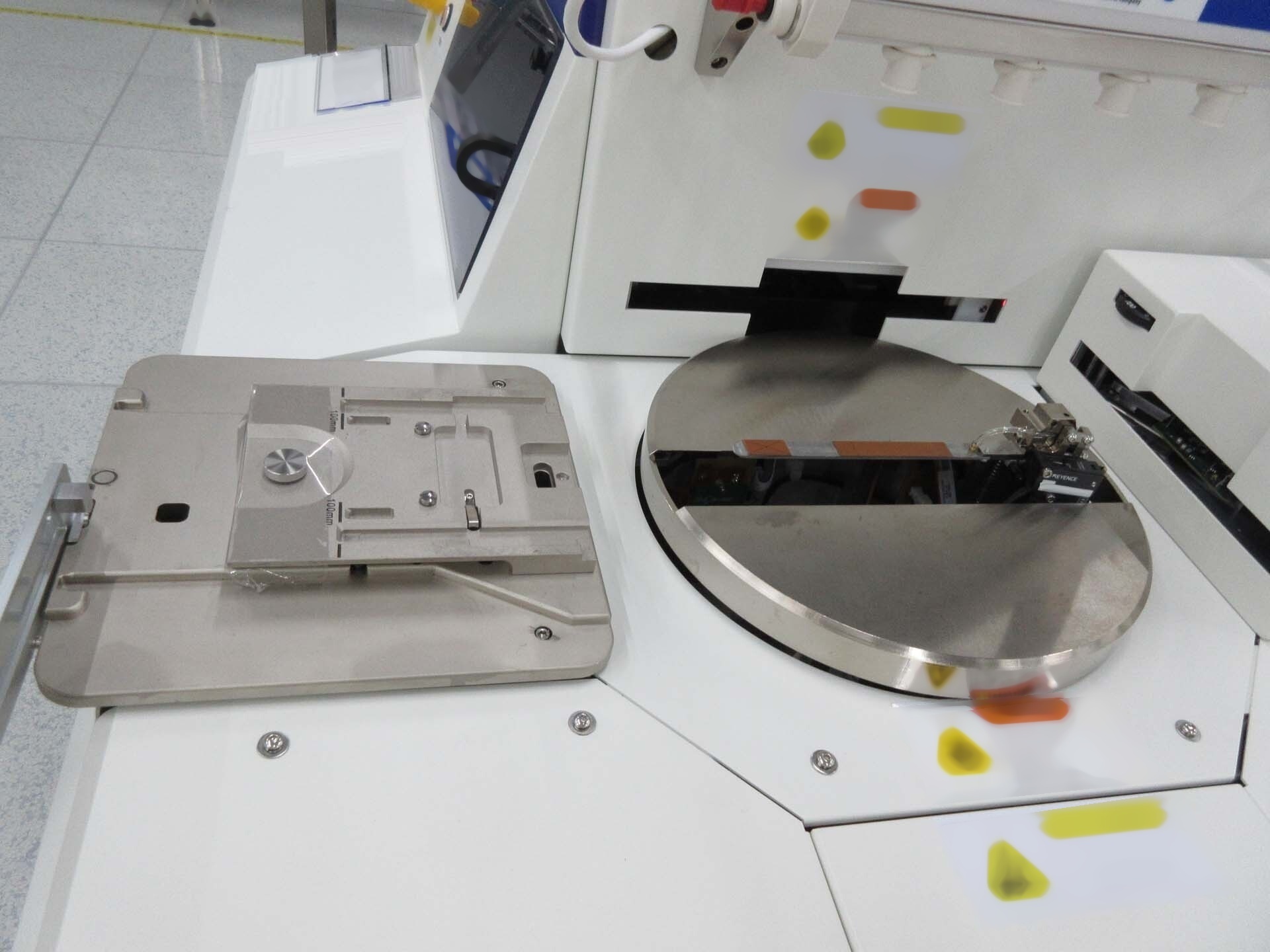
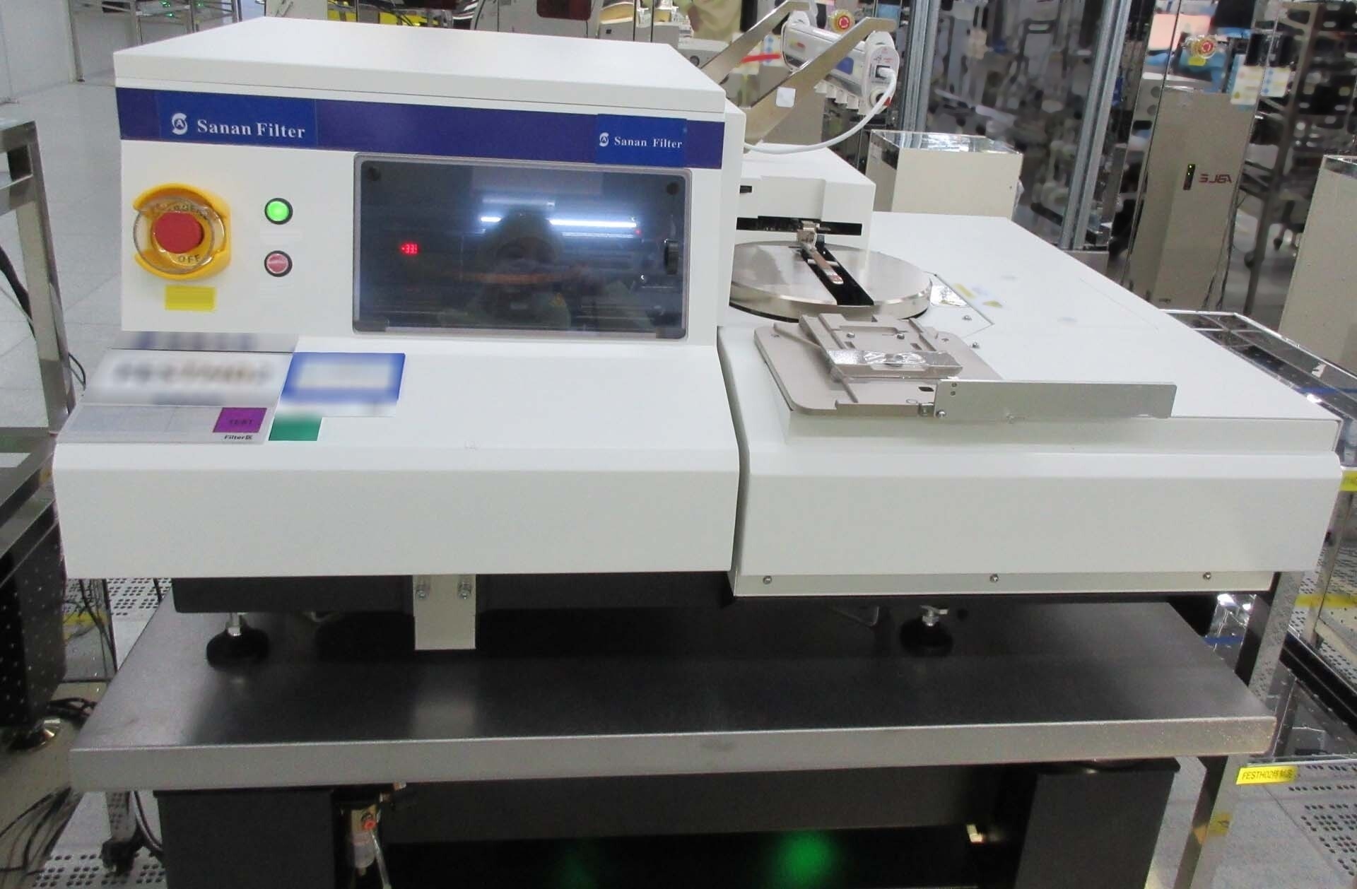
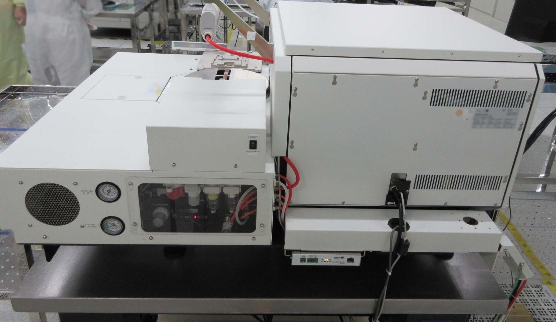
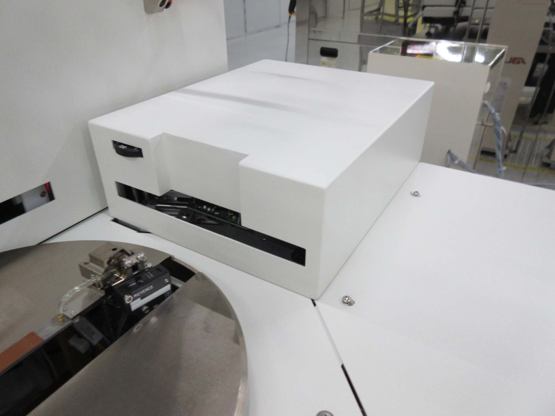
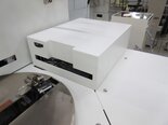
ID: 293799729
Vintage: 2020
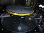
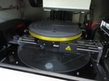
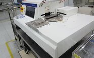
Surface profiler
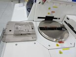
Chuck, 8"
Cassette, 8"
Wafer type: LT / BD / SI
SECS / GEM
Automatic transfer hander
Wafer thickness: 200 µm to 675 µm
Alignment for notch and flatted wafers
Constant stylus focus control
(5) Measurement heads
Monitor
Dual view optics (top and side)
Field of view: 850 x 1200 µm
Digital camera: 5 MP Color
Motorized level and theta axis
Stylus with radius: 2 µm
ProCal Wafer, 8"
Controller
Laser
Dongle
Operating system: Windows 7
PC
Manuals
2020 vintage.
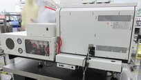
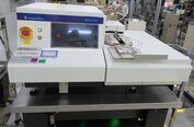
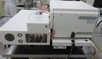
KLA / TENCOR P-170 is a wafer testing and metrology equipment designed for semiconductor and advanced materials research and development. It provides a comprehensive suite of test, measurement, and characterization capabilities, enabling materials researchers to quickly and accurately understand the electronic and structural properties of semiconductor and advanced materials. At the heart of the system is a novel 6-axis highly integrated scanning probe microscope (SPM), which combines nanometer scale resolution with a high precision scanner. This combination allows users to perform complex measurements on the entire surface of a wafer in a single scan, enabling quick and detailed analysis of material properties such as contact resistance, topography, and device performance. The unit also features a high-speed 3D profiling machine that uses a low-coherence laser source, coupled with a custom-designed hardware and software platform to acquire profiles of wafer features in seconds, providing an invaluable tool for the interactive detailing and visualization of nanometer-scale features. Additional features of KLA P-170 include advanced chip design and layout capabilities, integrated metrology algorithms, temperature-independent self-test routines, and a comprehensive suite of software for enhanced analysis. The intuitive graphical user interface simplifies the task of setting up, running, and analyzing data from the tool, allowing experienced and novice users alike to achieve accurate results with minimum effort. Overall, TENCOR P-170 builds on years of industry-leading research and development, providing users with powerful and reliable testing and metrology capabilities for semiconductor and advanced materials. From rapid wafer profiling to accurate and detailed pore analysis, P-170 provides unparalleled insight and resolution into the electronic and structural properties of materials.
There are no reviews yet