Used KLA / TENCOR P10 #293807273 for sale
URL successfully copied!
Tap to zoom
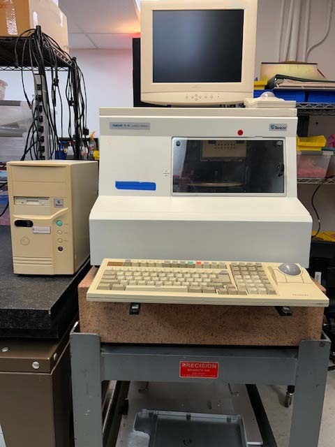

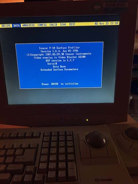
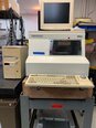
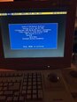
KLA / TENCOR P10 is a wafer testing and metrology equipment that is designed to provide high-performance and precision measurements of critical process parameters on semiconductor wafers during fabrication. It utilizes advanced laser, reflectometer, and scatterometry metrology techniques to collect extremely precise data at each individual processing step. This data is used to improve wafer production and yield as well as process control. KLA P-10 system is composed of a main subsystems: the main chamber, the optical table, the wafer-handling unit, the laser-source subsystem, the wafer sampling/measuring subsystem, and the data-translation subsystem. The main chamber houses the optical table and the wafer-handling machine, and it is optimized for a low temperature and low vibration operation. The optical table is constructed of optically flat ultra-low-mass granite and contains the wafer-sampling/measuring optics, such as the laser-source subsystem and a teledioptric tool. The laser-source subsystem consists of a laser, a reflectometer, and various detection optics. It is designed to collect precise data from the laser source on the wafers. The wafer-handling asset is a 12-axis motorized model with a fiber-optic coupler, which provides motion in all 6 directions and 3 angles. The wafer-sampling/measuring subsystem contains the wafer holder, the sample/measurement chamber, the light array, and several adjustable members. The light array is made of a series of lenses and light sources that are precisely detailed. The data-translation subsystem converts the measured data into structured information that can be analyzed for further process optimization. TENCOR P 10 equipment is designed to achieve high accuracy and repeatability. It is capable of analyzing various wafer depths from a few microns to several hundreds of microns, as well as providing uniformity measurements across the entire wafer. The advanced algorithms in P-10 system also enable precise wafer parameter mapping. The measuring unit is equipped with a 0.2 micron resolution imaging machine for exploring masks and systems. Overall, KLA P 10 wafer testing and metrology tool is designed to provide accurate and highly precise data on wafer processing parameters, allowing for greater process control and higher wafer yields. With its advanced laser, reflectometer, and scatterometry metrology techniques, this asset can provide a reliable and traceable record for semiconductor manufacturing.
There are no reviews yet